Switching control circuit and switching power-supply device
a control circuit and power supply technology, applied in the direction of electric variable regulation, process and machine control, instruments, etc., can solve the problems of hindering the cost reduction and achieve the effect of reducing the cost of the switching power supply devi
- Summary
- Abstract
- Description
- Claims
- Application Information
AI Technical Summary
Benefits of technology
Problems solved by technology
Method used
Image
Examples
first embodiment
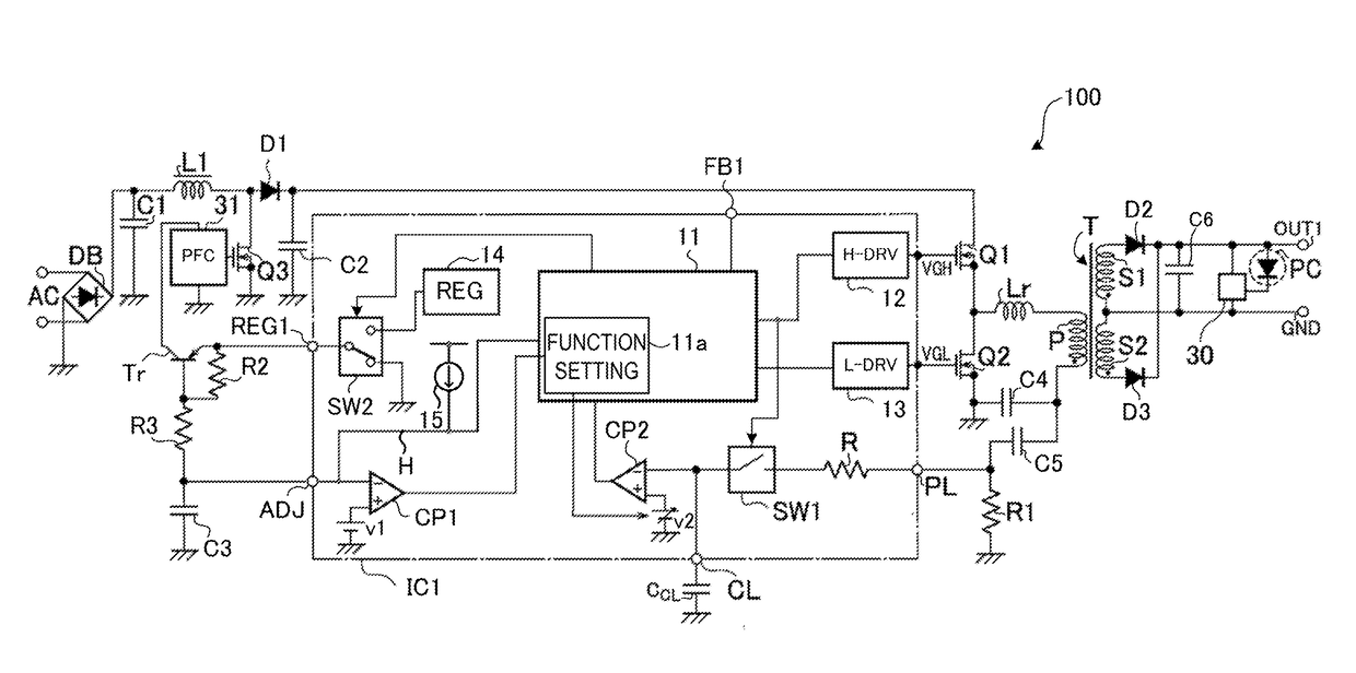
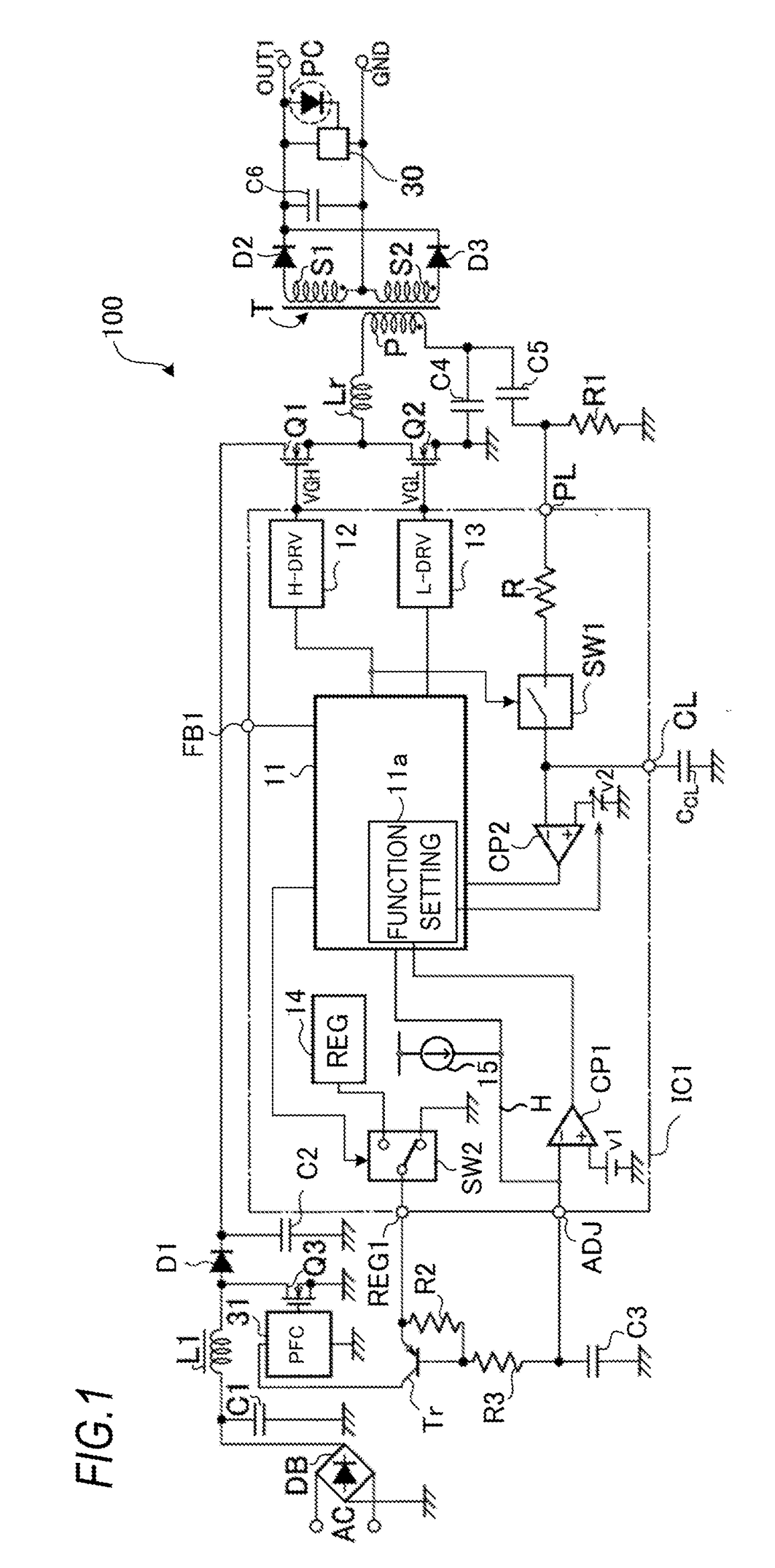
[0018]FIG. 1 is a view illustrating a schematic configuration of a current-resonance-type switching power-supply device according to a first embodiment of the present invention.
[0019]The switching power-supply device 100 illustrated in FIG. 1 includes a full-wave rectifier circuit DB, capacitors C1 to C6, inductors L1 and Lr, a PFC (Power Factor Correction) controller 31, switching elements Q1 to Q3, a transformer T having a primary coil P and secondary coils S1 and S2, diodes D1 to D3, a transistor Tr, resistor R1 to R3, a photo coupler PC, an output voltage detector 30, a capacitor CCL, and a switching control circuit IC1.
[0020]The full-wave rectifier circuit DB performs the full-wave rectification of an AC voltage AC and outputs a full-wave rectified voltage.
[0021]One end of the inductor L1 is connected to an output terminal of the full-wave rectifier circuit DB. An anode of the diode D1 is connected to the other end of the inductor L1. A series circuit of the switching elements ...
second embodiment
[0069]FIG. 3 is a view illustrating a schematic configuration of a DC / DC converter 200 of a switching power-supply device according to the second embodiment of the present invention.
[0070]The DC / DC converter 200 includes a switching control circuit IC2 constituted by an integrated circuit, resistors R4 to R6, a bootstrap capacitor C7, a capacitor C8, and an inductor L2.
[0071]One end of the resistor R4 is connected to an external terminal BS of the switching control circuit IC2. The other end of the resistor R4 is connected to one end of the bootstrap capacitor C7. The other end of the bootstrap capacitor C7 is connected to an external terminal SW of the switching control circuit IC2.
[0072]The external terminal SW constitutes a first external terminal. The external terminal BS constitutes a second external terminal. The bootstrap capacitor C7 constitutes a passive element.
[0073]One end of the inductor L2 is connected to a connecting point between the external terminal SW of the switc...
third embodiment
[0100]FIG. 4 is a view illustrating a schematic configuration of an LED backlight driver 300, in which the switching control circuit of the present invention is applied.
[0101]The LED backlight driver 300 includes a switching control circuit IC3 constituted by an integrated circuit, and pull-up resistors Rp1 and Rp2.
[0102]One end of the pull-up resistor Rp1 is connected to an external terminal PWM1 of the switching control circuit IC3. The external terminal PWM1 is a terminal for inputting a signal of 0 or 1 for the lighting control of the LED. The external terminal PWM1 constitutes a second external terminal.
[0103]The other end of the pull-up resistor Rp1 is connected to an external terminal REG2 of the switching control circuit IC3. The external terminal REG2 is a terminal for outputting voltage to an outside of the switching control circuit IC3. The external terminal REG2 constitutes a first external terminal.
[0104]One end of the pull-up resistor Rp2 is connected to an external te...
PUM
 Abstract
Description
Claims
Application Information


