
Sgt mosfet with adjustable crss and ciss

a technology of mosfet and crss, which is applied in the direction of basic electric elements, electrical apparatus, semiconductor devices, etc., can solve the problems of low crss, high turning, technical limitations, etc., and achieve the effect of flexible adjustment of the connection configuration and reducing the ringing

Active Publication Date: 2017-06-08
HUNTECK SEMICON (SHANGHAI) LTD
View PDF2 Cites 12 Cited by
  • Summary
  • Abstract
  • Description
  • Claims
  • Application Information

AI Technical Summary

Benefits of technology

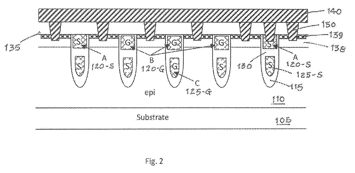
The present invention provides a new and improved semiconductor power device with the shielded gate trench structure that allows flexible adjustment of the connections of the bottom electrodes. Specifically, some of the bottom-shielding electrodes are connected to the source metal and some of the bottom shielding electrodes connected to the gate metal. By adjusting the ratio of the source and gate connections of the bottom electrodes, the Crss can be flexibly adjusted to achieve different design goals for different types of applications. This new configuration helps to reduce ringing and avoid EMI issues in power devices for DC-DC applications.

Problems solved by technology

However, a power device with a lower CRSS may lead to other technical limitations such as issues caused by high gate ringing, high turning on and turning off VDS spikes, and electromagnetic interference (EMI).
Furthermore, conventional technologies for manufacturing the SGT MOSFET encounter another difficulty due to the requirement of reducing the specific-on resistance in a device that has a high cell density with significantly reduced pitch.
The high density configurations with reduced pitch often causes the input capacitance CISS o increase thus slowing down the tuning on and off speeds.
Additionally, high CISS also leads to higher switch loss, increased gate charges thus requiring a stronger gate drive.
For these reasons, the conventional SGT MOSFET devices are limited by a tradeoff between the needs to reduce the specific-on resistance and the undesirable result of increasing the CISS.
Even the device configuration has the benefits of reduced gate to drain capacitance; however, as discussed above, there are limitations and difficulties with such device configuration.

Method used


Image

  • Sgt mosfet with adjustable crss and ciss
  • Sgt mosfet with adjustable crss and ciss
  • Sgt mosfet with adjustable crss and ciss

Examples


Embodiment Construction

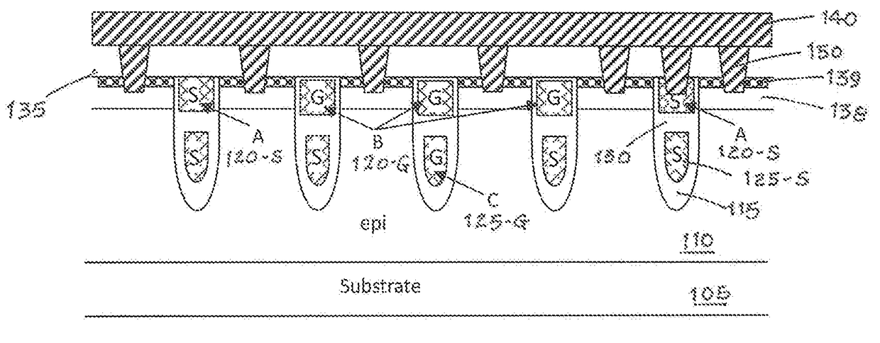
[0022]Referring to FIG. 2 that shows a cross sectional view of a portion of a shielded gate trench (SGT) MOSFET 100 as an embodiment of this invention. The shielded gate trench (SGT) MOSFET power device 100 as shown is formed in a semiconductor wafer that includes epitaxial layer 110 supported on a heavily doped bottom substrate 105. The epitaxial layer 110 may include one, two or even more doping concentration sublayers. In the active cell area of the device 100 as shown, the device 100 includes a plurality of shield gate trenches 115 padded by a gate oxide layer 118. In each of the shield gate trenches there is a top electrode 120 and bottom electrode 125 shielded by a dielectric layer 130 disposed between the top electrode and the bottom electrode 125. Unlike the conventional shield gate trenches, some of the bottom electrodes 125-S are electrically connected to source and some other bottom electrodes 125-G are electrically connected to gate as that shown in location C in FIG. 2....


PUM


Abstract

A semiconductor power device includes a plurality of power transistor cells each having a trenched gate disposed in a gate trench opened in a semiconductor substrate wherein a plurality of the trenched gates further include a shielded bottom electrode disposed in a bottom portion of the gate trench electrically insulated from a top gate electrode disposed at a top portion of the gate trench by an inter-electrode insulation layer. At least one of the shielded bottom electrode is connected a source metal and at least one of the top electrodes in the gate trench is connected to a source metal of the power device.

Description

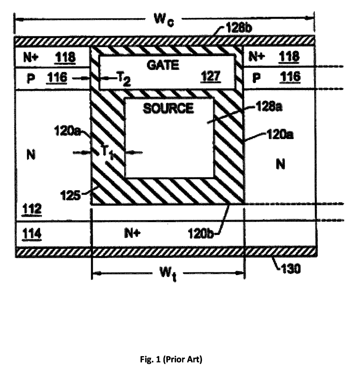
BACKGROUND OF THE INVENTION[0001]1. Field of the Invention[0002]This invention relates generally to structural configurations and manufacturing methods of the semiconductor power devices. More particularly, this invention relates to improved device configurations and manufacturing processes to flexibly adjust device characteristics of Crss and Ciss to smooth the waveforms and to avoid electromagnetic interference (EMI) in the shield gate trench (SGT) MOSFET.[0003]2. Description of the Prior Art[0004]The conventional technologies for reducing the gate to drain capacitance in a power semiconductor device is achieved by implementing a shielded gate trench (SGT) configuration. Comparing with the traditional trench gate MOSFET, the split gate structure has the advantage of lowering CRSS thus achieving much better efficiency. Specifically, a power MOSFET with a lower CRSS has the advantages of high switching speed and a lower loss. However, a power device with a lower CRSS may lead to oth...

Claims


Application Information

Patent Timeline
Patent Type & Authority Applications(United States)
IPC IPC(8): H01L29/78H01L21/3213H01L29/40H01L29/66H01L29/10
CPCH01L29/7813H01L29/66734H01L21/32139H01L29/7811H01L29/401H01L29/1095H01L29/407H01L29/42372
Inventor HU, JUNLUO, ZHIYUNWANG, FEIPAN, MENGYU
Owner HUNTECK SEMICON (SHANGHAI) LTD
Learn More