Defect signal to noise enhancement by reducing die to die process noise

a technology of noise enhancement and defect signal, applied in the field of image processing, can solve problems such as difficulty in finding defects, difficulty in correcting color variation or noise, and inability to identify the best mode of defect inspection

Active Publication Date: 2017-06-15
KLA CORP
View PDF3 Cites 19 Cited by
  • Summary
  • Abstract
  • Description
  • Claims
  • Application Information

AI Technical Summary

Problems solved by technology

It is difficult to correct color variation or noise.
This can make it impossible to identify the best mode for defect inspection because the defect cannot be seen in the color noise.
Process variation can make it difficult to find defects and may result in false positives.
Increasing tolerance in a histogram can result in loss of some of the defects.

Method used


Image

  • Defect signal to noise enhancement by reducing die to die process noise
  • Defect signal to noise enhancement by reducing die to die process noise
  • Defect signal to noise enhancement by reducing die to die process noise

Examples


Embodiment Construction

[0029]Although claimed subject matter will be described in terms of certain embodiments, other embodiments, including embodiments that do not provide all of the benefits and features set forth herein, are also within the scope of this disclosure. Various structural, logical, process step, and electronic changes may be made without departing from the scope of the disclosure. Accordingly, the scope of the disclosure is defined only by reference to the appended claims.

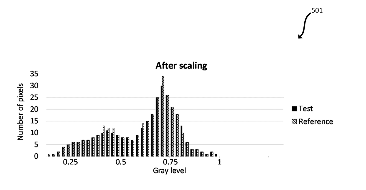
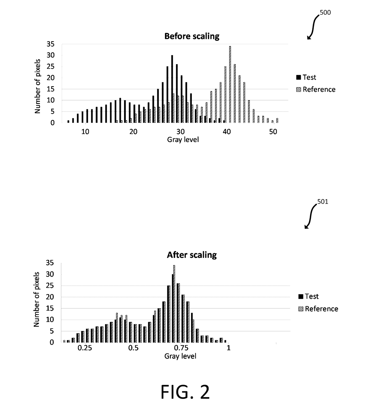
[0030]It may be difficult to detect a particular defect of interest (DOI) because it is “buried” by process variation. Embodiments disclosed herein can reduce or eliminate process variation before a difference image is generated. The techniques disclosed herein can achieve color noise reduction by adjusting the background gray level of a reference image to an image of part of a wafer (e.g., a defect image or test image). This enhances sensitivity to the DOI. For example, the techniques disclosed herein provide improved de...


PUM


Abstract

Gray level histograms for a test image and a reference image are adjusted by histogram scaling. Parameters from the histogram scaling are applied to the test image and the reference image. After the parameters are applied, the reference image and the test image are compared to produce a difference image, such as by subtracting the reference image from the test image. Noise in the difference image can be reduced, which improves defect identification in the difference image. In addition, noisy structures in the difference image which are elongated in vertical or horizontal direction can be found. If the noise exceeds a certain threshold, the structures may not be inspected.

Description

CROSS-REFERENCE TO RELATED APPLICATIONS[0001]This application claims priority to the provisional patent application filed Dec. 9, 2015 and assigned U.S. App. No. 62 / 265,019, the disclosure of which is hereby incorporated by reference.FIELD OF THE DISCLOSURE[0002]This disclosure relates to image processing.BACKGROUND OF THE DISCLOSURE[0003]Wafer inspection systems help a semiconductor manufacturer increase and maintain integrated circuit (IC) chip yields by detecting defects that occur during the manufacturing process. One purpose of inspection systems is to monitor whether a manufacturing process meets specifications. The inspection system indicates the problem and / or the source of the problem if the manufacturing process is outside the scope of established norms, which the semiconductor manufacturer can then address.[0004]Evolution of the semiconductor manufacturing industry is placing ever greater demands on yield management and, in particular, on metrology and inspection systems....

Claims


Application Information

Patent Timeline
Patent Type & Authority Applications(United States)
IPC IPC(8): G06T5/40
CPCG06T2207/10061G06T5/40G06T2207/30148G06T7/001G01N27/04G01N2223/6116
Inventor BRAUER, BJORNSMITH, JAMES A.
Owner KLA CORP
Why Eureka
Try Eureka