Accelerated characterization of circuits for within-die process variations

a technology of process variations and circuits, applied in the field of timing analysis of integrated circuit designs, can solve the problems of less yield, increased parasitic resistance, and more defects in circuits placed near the edge of integrated circuit dies, and achieve the effect of efficiently determining sensitivity and timing variations

Active Publication Date: 2014-08-19
CADENCE DESIGN SYST INC
View PDF11 Cites 12 Cited by
  • Summary
  • Abstract
  • Description
  • Claims
  • Application Information

AI Technical Summary

Problems solved by technology

For example, circuits that are placed near an edge of the integrated circuit die may have more defects and lower yield than circuits placed near the center of a die.
A thinner metal signal line may generate a greater parasitic resistance and slow down signal transmission.
A thinner metal power line may reduce its current carrying capabilities and result in a power failure.
A thinner dielectric layer may result in increased parasitic capacitance between metal layers and the metal lines formed therein and reduce the speed of signal transmission.

Method used


Image

  • Accelerated characterization of circuits for within-die process variations
  • Accelerated characterization of circuits for within-die process variations
  • Accelerated characterization of circuits for within-die process variations

Examples


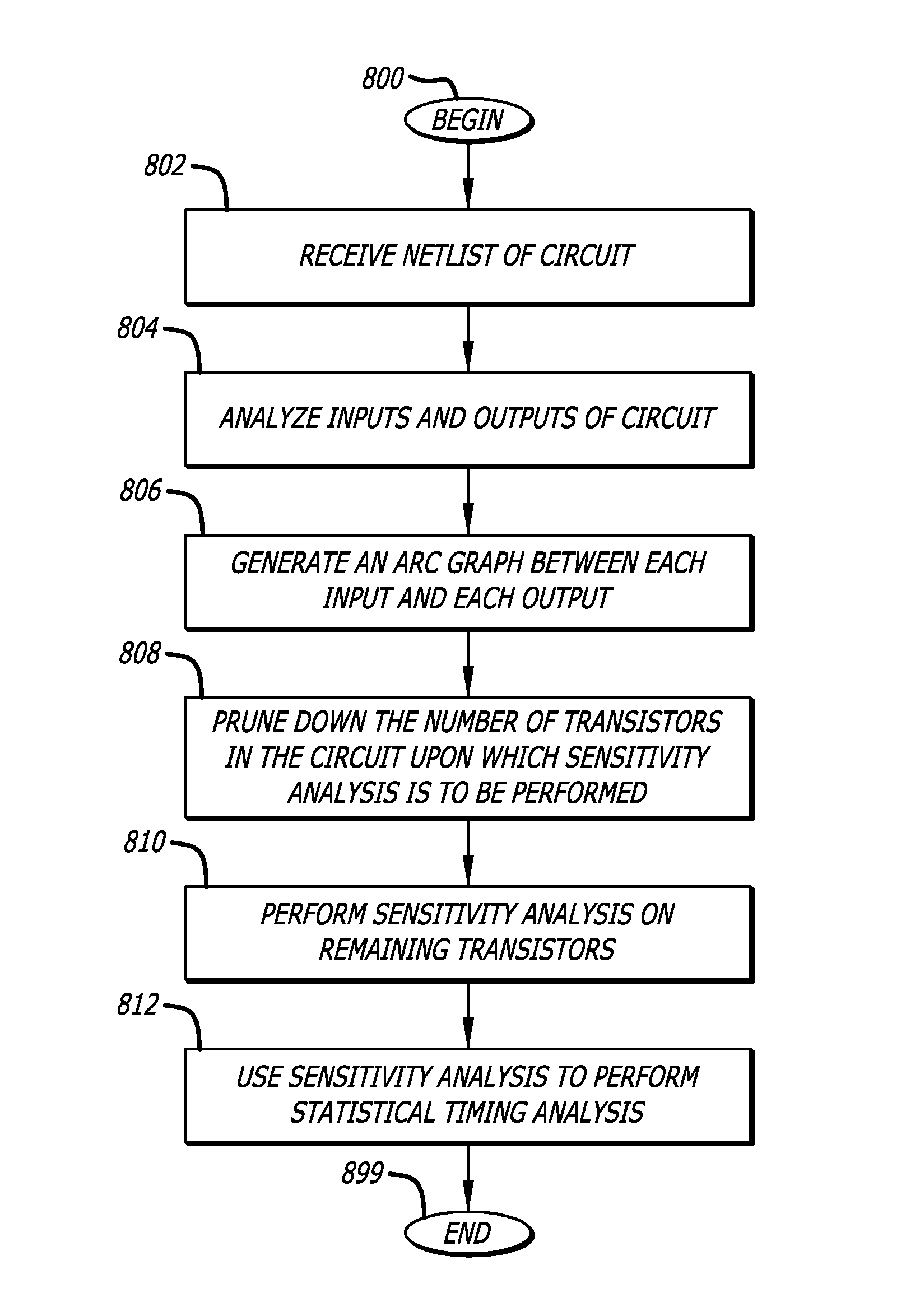
Embodiment Construction

[0034]In the following detailed description of the embodiments of the invention, numerous specific details are set forth in order to provide a thorough understanding of the embodiments of the invention. However, the embodiments of the invention may be practiced without these specific details. In other instances well known methods, procedures, components, and circuits have not been described in detail so as not to unnecessarily obscure aspects of the embodiments of the invention.
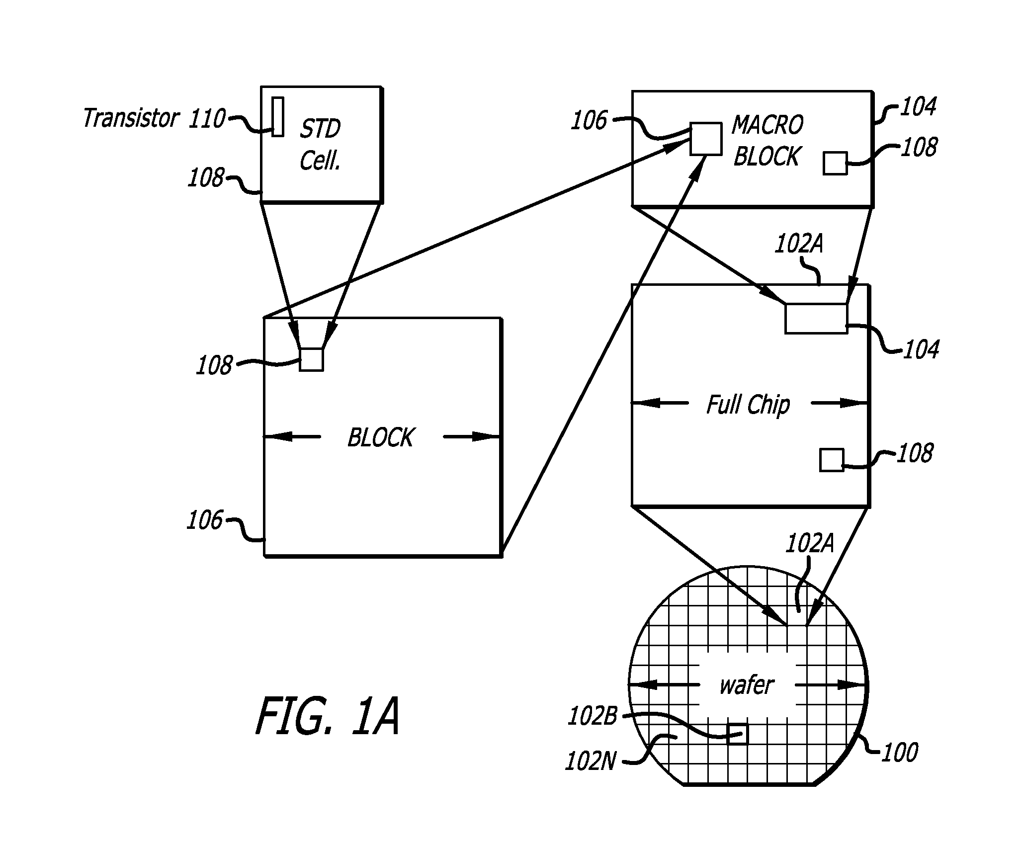
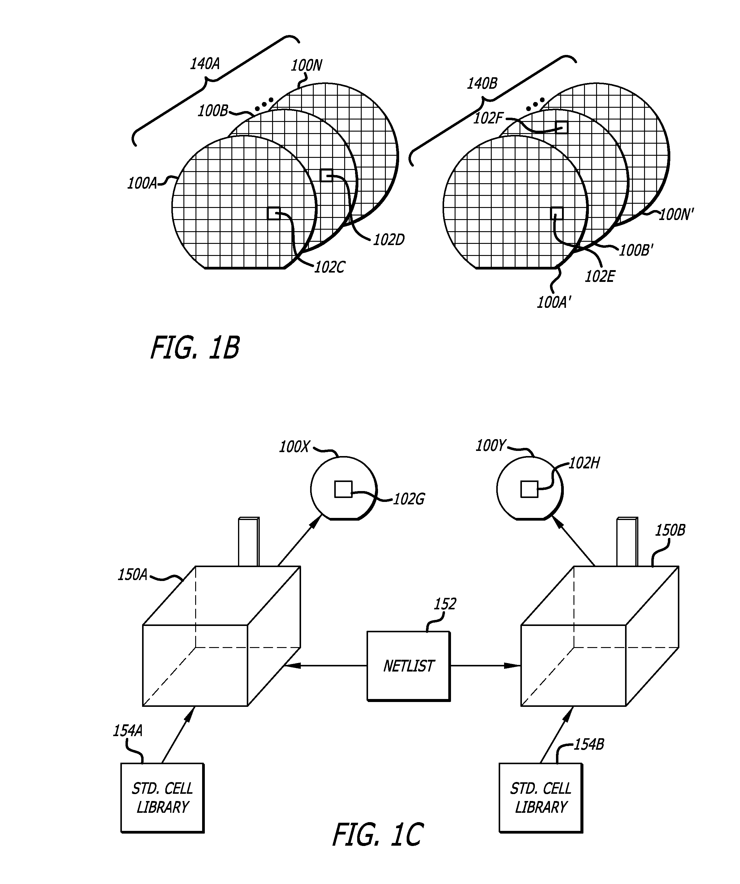
Introduction

[0035]Conventional static timing analysis (STA) using best case / worst case analysis is usually overly pessimistic but may also be too optimistic in some cases. This has resulted in the promotion of statistical static timing analysis (SSTA) over conventional static timing analysis as a method for estimating yield of a circuit in terms of timing activities.

[0036]The accuracy of statistical static timing analysis is directly related to the accuracy and availability of statistical information in the t...


PUM


Abstract

In one embodiment of the invention, a method for electronic circuit design is disclosed. The method includes analyzing a netlist of a subcircuit to determine one or more input pins and one or more output pins; forming an arc graph of the subcircuit including one or more timing arcs between the one or more input pins and the one or more output pins; and reducing the number of transistors to perturb to perform a sensitivity analysis for within die process variations over the one or more timing arcs to reduce the number of simulations to characterize the subcircuit.

Description

FIELD[0001]The embodiments of the invention relate generally to timing analysis of integrated circuit designs.BACKGROUND[0002]Design parameters for an integrated circuit may vary wafer lot to waver lot, from wafer to wafer within lot, from die to die on a wafer, and within die of an integrated circuit.[0003]Referring now to background FIG. 1A, a wafer 100 is illustrated with a plurality of integrated circuit die 102A-102N formed therein in a matrix or rows and columns. FIG. 1A further illustrates a hierarchy of circuitry that may be used to define an integrated circuit die 102A. Each complete integrated circuit (“full chip”) die 102A may include macro functional blocks 104 as well as lower level blocks and circuit cells. The macro functional blocks 104 for example may be processors, memory, or other types of functional blocks. The macro functional blocks 104 may be made of other smaller functional blocks 106 grouped together. The functional blocks 106, for example, may be registers,...

Claims


Application Information

Patent Timeline
Patent Type & Authority Patents(United States)
IPC IPC(8): G06F17/50
CPCG06F17/50G06F17/5031G06F2217/12G06F17/5081G06F2217/84G06F30/3312G06F2119/18G06F30/398G06F2119/12Y02P90/02
Inventor PARAMESWARAN, HARINDRANATHSHRIVASTAVA, SACHIN
Owner CADENCE DESIGN SYST INC
Why Eureka
Try Eureka