Single crystal copper bonding lead and preparation method thereof

A technology for bonding wires and single crystal copper, which is applied in the field of microelectronic material production, can solve problems such as difficulty in being used, and achieve the effects of eliminating lateral grain boundaries, stable performance, and overcoming many broken ends.

Inactive Publication Date: 2012-08-15
宋东升
View PDF3 Cites 12 Cited by
  • Summary
  • Abstract
  • Description
  • Claims
  • Application Information

AI Technical Summary

Problems solved by technology

In this way, it is obviously difficult to realize the multi-layer interconnection on the silicon chip due to the high resistivity of aluminum.

Method used


Image

  • Single crystal copper bonding lead and preparation method thereof
  • Single crystal copper bonding lead and preparation method thereof

Examples


Embodiment

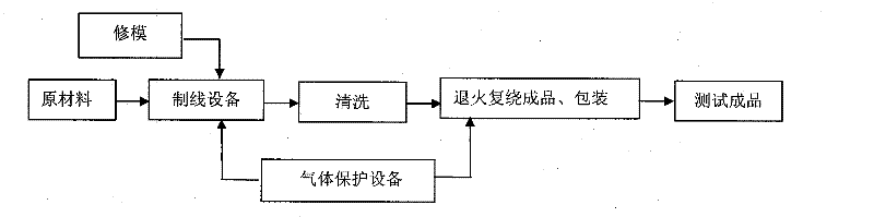
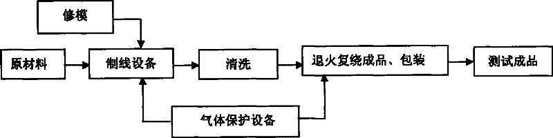
[0015] Embodiment: Step 1: Use ultrasonic mold repairing equipment to trim molds as needed, and use high-purity argon protection equipment with a purity of over 99.99% in the process of wire making and annealing and rewinding finished products; Step 2: The equipment is the key Lead wire drawing machine, the vacuum degree is 10-104MPa High-vacuum furnace melts high-purity copper with a purity higher than 99.995%, heats up to 1100-1180°C, and refines for 60-120 minutes. The entire melting process uses high-purity copper with a purity of more than 99.99%. Pure argon protection, and directional solidification method to draw Φ4 ~ Φ8mm single crystal copper rod; the third step: the equipment is bonding wire medium drawing machine, small drawing machine, fine drawing machine, micro drawing machine. The drawn high-purity single crystal copper rod is cold processed to Φ0.95~Φ1.102mm, the drawing processing rate of each pass is 15~25%, and the drawing speed is controlled at 40~60m / min; t...


PUM


Abstract

The invention discloses a single crystal copper bonding lead and a preparation method thereof, relating to the field of production of microelectronic materials. The production technology integrates a metal material preparation process, a heat treatment process and a diamond die process, ensures the production consistency and reliability and realizes the large-scale production. The adopted production process comprises the steps of providing die repair and gas protection equipment, smelting, wiredrawing, cleaning, and compounding, packaging and testing a finished product. The single crystal copper bonding lead has the beneficial effects that as a signal crystal copper material has a compact solidification structure, lateral crystal boundaries are eliminated, the casting defects of shrinkage cavities, pores and the like are avoided, the plastic working performance, the mechanical performance, the electric performance and the like of the signal crystal copper material are obviously higher than those of the conventional oxygen-free copper, the defects of more end breakage, low quality and low productivity in the wiredrawing process of the conventional copper wire are overcome, and an electronic packaging bonding wire with the wire diameter reaching 0.015m, high strength, high elongation and stable performance can be prepared.

Description

technical field [0001] The invention relates to the field of microelectronic material production, in particular to a single crystal copper bonding wire and a preparation method thereof. Background technique [0002] With the vigorous development of the microelectronics industry, the integrated circuit electronic packaging industry is rapidly advancing towards the direction of small size, high performance, high density, and multi-chip, so the requirements for the lead material of the integrated circuit package are very fine (Φ0.016mm), and The ultra-fine bonding gold wire can no longer meet the requirements of narrow-pitch and long-distance bonding technical indicators in the bonding process. In the ultra-fine-pitch spherical bonding process, due to the increase in the number of package pins and the reduction of the pin pitch, the ultra-fine bonding gold wire often causes the swing of the bonding wire, bonding breakage and wire stepping during the bonding process. Phenomenon...

Claims


Application Information

Patent Timeline
Patent Type & Authority Applications(China)
IPC IPC(8): H01L23/48H01B1/02
CPCH01L24/43H01L2224/43H01L2224/43848H01L2224/45H01L2224/45015H01L2224/45144H01L2224/45147H01L2924/00014H01L2924/01006H01L2924/30107H01L2924/00H01L2224/48H01L2924/2011H01L2924/00012
Inventor 宋东升
Owner 宋东升
Why Eureka
Try Eureka