Multi-layer stamp

a multi-layer stamp and stamping technology, applied in the field of stamps, can solve the problems of difficult to pick up and place ultra-thin, fragile or small devices using such conventional technologies, and the conventional method of applying integrated circuits to a destination substrate is limited to relatively large devices

Active Publication Date: 2017-06-22
X DISPLAY CO TECH LTD
View PDF6 Cites 28 Cited by
  • Summary
  • Abstract
  • Description
  • Claims
  • Application Information

AI Technical Summary

Benefits of technology

[0021]It can be desirable to transfer as many devices with a micro-transfer printing stamp as possible and it is therefore desirable to use a stamp that is large and has many posts. However, as structures become larger, it is increasingly difficult to make them with fine precision. It is an advantage of the present invention that larger micro-transfer printing stamps with more posts are made with improved precision and flat surfaces suitable for micro-transfer printing from relatively larger substrates, such as semiconductor substrates. This is accomplished by providing one or more intermediate pedestal layers between the stamp posts and the support. The cured intermediate pedestal layers provide increasing flatness over the support so that the distal ends of the stamp posts across the extent of the stamp are more closely aligned in a plane.
[0022]In another embodiment of the present invention, the stamp for micro-transfer printing of the present invention is made by a process of the present invention and used for micro transfer printing by pressing the non-planar surface at the distal end of one of the one or more posts against the non-planar contact surface of the micro-transfer printable device to adhere the micro-transfer printable device to the distal end of the one post, removing the micro-transfer printable device from the wafer with the stamp, pressing the micro-transfer printable device to a destination substrate with the stamp to adhere the micro-transfer printable device to the destination substrate, and removing the stamp from the micro-transfer printable device and the destination substrate.
[0023]In one aspect, the disclosed technology includes a stamp for micro-transfer printing, including: a support having a support stiffness and a support coefficient of thermal expansion (CTE); a pedestal layer formed on the support, the pedestal layer having a pedestal layer stiffness that is less than the support stiffness and a pedestal layer coefficient of thermal expansion (CTE) that is different from the support coefficient of thermal expansion (CTE); and a stamp layer formed on the pedestal layer, the stamp layer having a body and one or more protrusions extending from the body in a direction away from the pedestal layer, the stamp layer having a stamp layer stiffness that is less than the support stiffness and a stamp layer coefficient of thermal expansion that is different from the support coefficient of thermal expansion.
[0024]In certain embodiments, the pedestal layer is made of the same material as the stamp layer or wherein the pedestal layer comprises the same materials as the stamp layer but in different proportions.
[0025]In certain embodiments, at least one of the pedestal layer and the stamp layer is polydimethylsiloxane (PDMS).
[0026]In certain embodiments, the support is glass, metal, or ceramic.

Problems solved by technology

Conventional methods such as pick-and-place for applying integrated circuits to a destination substrate are limited to relatively large devices, for example having a dimension of a millimeter or more and it is often difficult to pick up and place ultra-thin, fragile, or small devices using such conventional technologies.

Method used


Image

  • Multi-layer stamp
  • Multi-layer stamp
  • Multi-layer stamp

Examples


Embodiment Construction

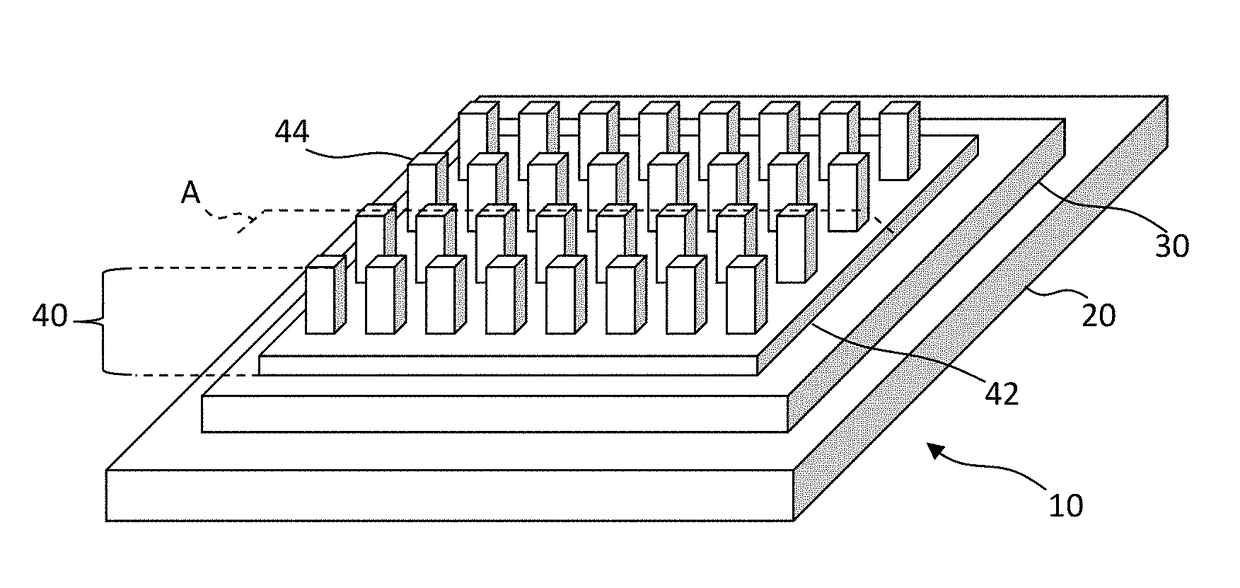
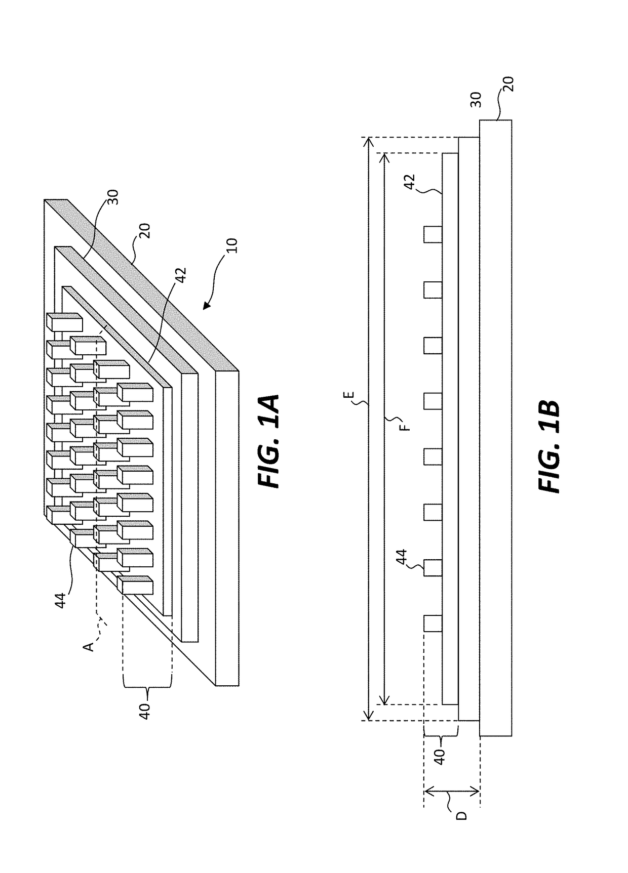
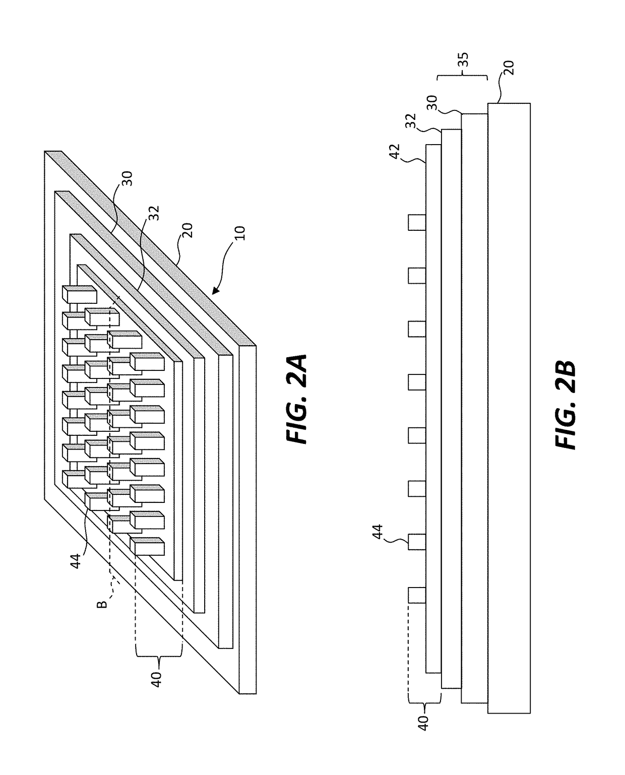
[0064]The present invention provides a stamp and methods of making the stamp for micro-transfer printing micro-transfer printable devices. The micro-transfer printable devices can be light emitters or integrated circuits, for example CMOS integrated circuits made on or in a silicon semiconductor wafer, light-emitting diodes (LEDs), for example made on or in a GaN semiconductor material, or silicon photodiodes. The wafers can have a diameter, for example, greater than or equal to 10 cm, 15 cm, 20 cm, 25 cm, 30 cm, 40 cm, 100 cm, or even larger. The micro-transfer printable devices can have, for example, a width from 1-8 μm, a length from 5-10 μm, or a height from 0.5-3 μm. More generally, the micro-transfer printable devices can include or be a variety of chiplets having conductor or semiconductor structures, including a diode, a light-emitting diode (LED), a transistor, a laser, active electrical components, passive electrical components, or an electrical jumper.

[0065]Chiplets are s...


PUM

PropertyMeasurementUnit
diameteraaaaaaaaaa
diameteraaaaaaaaaa
diameteraaaaaaaaaa

Abstract

A stamp for micro-transfer printing includes a support having a support stiffness and a support coefficient of thermal expansion (CTE). A pedestal layer is formed on the support, the pedestal layer having a pedestal layer stiffness that is less than the support stiffness and a pedestal layer coefficient of thermal expansion (CTE) that is different from the support coefficient of thermal expansion (CTE). A stamp layer is formed on the pedestal layer, the stamp layer having a body and one or more protrusions extending from the body in a direction away from the pedestal layer. The stamp layer has a stamp layer stiffness that is less than the support stiffness and a stamp layer coefficient of thermal expansion that is different from the support coefficient of thermal expansion.

Description

CROSS REFERENCE TO RELATED APPLICATION[0001]This application is related to U.S. patent application Ser. No. 14 / 804,031 filed Jul. 20, 2015, entitled Apparatus and Methods for Micro-Transfer-Printing, and to U.S. patent application Ser. No. 14 / 918,174 filed Oct. 20, 2015, entitled Stamp with Structured Posts, which are hereby incorporated by reference in their entirety.FIELD OF THE INVENTION[0002]The present invention relates to stamps used in micro transfer printing.BACKGROUND OF THE INVENTION[0003]The disclosed technology relates generally to methods and tools for micro-transfer-printing. Conventional methods such as pick-and-place for applying integrated circuits to a destination substrate are limited to relatively large devices, for example having a dimension of a millimeter or more and it is often difficult to pick up and place ultra-thin, fragile, or small devices using such conventional technologies. More recently, micro-transfer printing methods have been developed that permi...

Claims


Application Information

Patent Timeline
Patent Type & Authority Applications(United States)
IPC IPC(8): B29C59/02B29C59/00
CPCB29C59/026B29L2007/001B29C59/002B29C59/02B29C2059/023B29C2059/028B41F17/00B29L2031/34H01L2224/75305H01L2224/75621H01L24/75H01L2224/81201H01L2224/13013H01L2224/13016H01L24/81H01L21/7806H01L25/0753H01L33/0095H01L2224/16227H01L2924/00014H01L33/0093H01L2224/13099H01L2224/81345H01L2224/81005H01L2224/81986H01L2224/81901B41F16/00H01L21/6835H01L24/95B29C33/3842
Inventor MOORE, TANYA YVETTECOK, RONALD S.GOMEZ, DAVID
Owner X DISPLAY CO TECH LTD
Why Eureka
Try Eureka