Method, image processing system and computer-readable recording medium for item defect inspection

Active Publication Date: 2017-06-29
POWERCHIP SEMICON MFG CORP
View PDF19 Cites 16 Cited by
  • Summary
  • Abstract
  • Description
  • Claims
  • Application Information

AI Technical Summary

Benefits of technology

[0005]Accordingly, the disclosure is directed to a method, an image processing system, and a computer-readable recording medium

Problems solved by technology

For example, during a wafer manufacturing process, defects could occur on wafer surfaces due to equipments, environment, and human causes.
However, when color cast, color shift, uneven brightness, or nois

Method used


Image

  • Method, image processing system and computer-readable recording medium for item defect inspection
  • Method, image processing system and computer-readable recording medium for item defect inspection
  • Method, image processing system and computer-readable recording medium for item defect inspection

Examples


Embodiment Construction

[0021]Some embodiments of the disclosure will now be described more fully hereinafter with reference to the accompanying drawings, in which some, but not all embodiments of the application are shown. Indeed, various embodiments of the disclosure may be embodied in many different forms and should not be construed as limited to the embodiments set forth herein; rather, these embodiments are provided so that this disclosure will satisfy applicable legal requirements. Like reference numerals refer to like elements throughout.

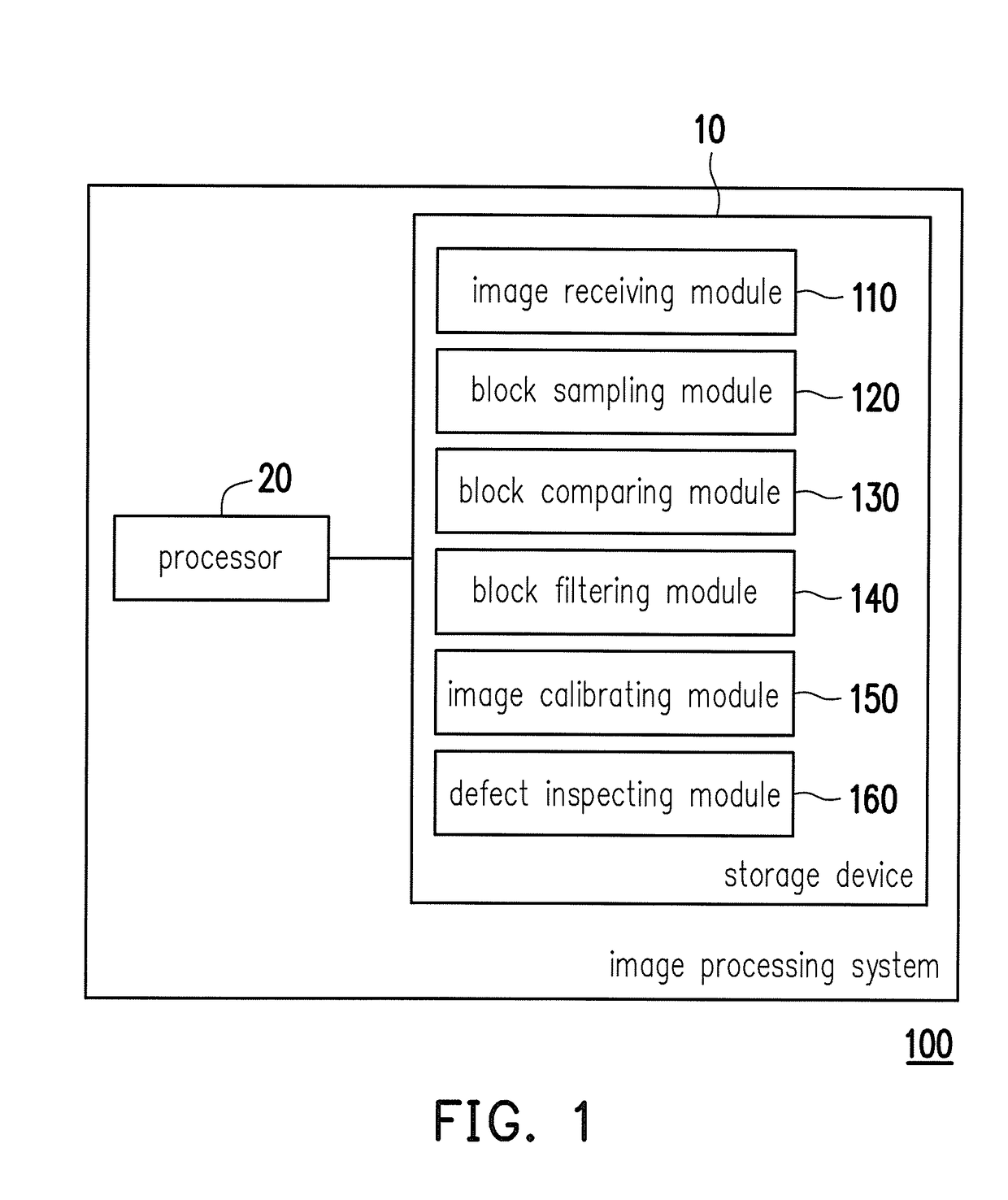
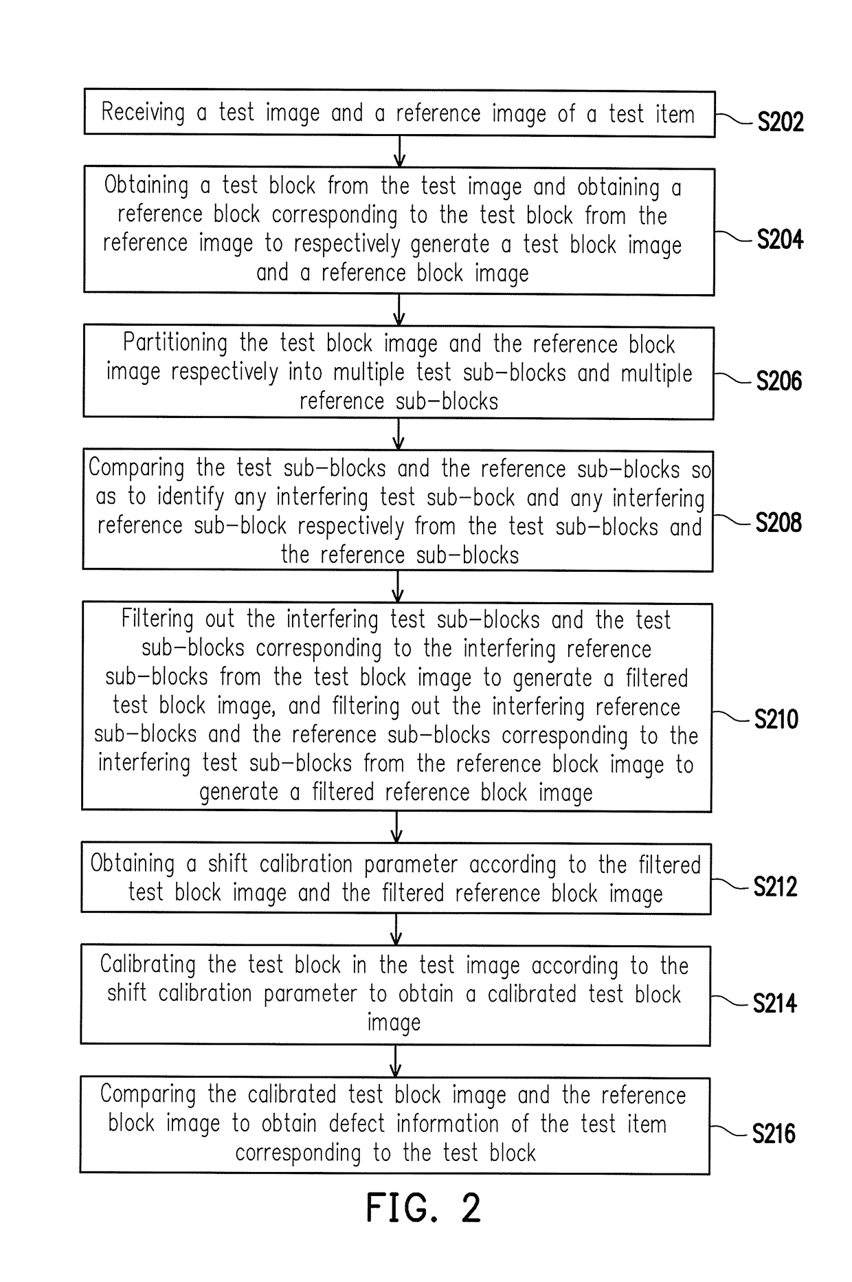
[0022]FIG. 1 illustrates a block diagram of an image processing system according to an embodiment of the disclosure. It should, however, be noted that this is merely an illustrative example and the disclosure is not limited in this regard. All components of the image processing system and their configurations are first introduced in FIG. 1. The detailed functionalities of the components are disclosed along with FIG. 2.

[0023]Referring to FIG. 1, an image processing s...


PUM


Abstract

A method, image processing system, and computer-readable recording medium for item defect inspection are provided. The method is as follows. A test image and a reference image of a test item are received. A test block and a corresponding reference block are obtained from the test image and the reference image to generate a test block image and a reference block image. The test block image and the reference block image are respectively partitioned into multiple sub-blocks. All interfering sub-blocks are identified and filtered out from the test block image and the reference block image, and a shift calibration parameter is obtained accordingly. The test block in the test image is calibrated based on the shift calibration parameter to generate a calibrated test block image. The calibrated test block image and the reference block image are compared to obtain defect information of the test item corresponding to the test block.

Description

CROSS-REFERENCE TO RELATED APPLICATION[0001]This application claims the priority benefit of Taiwan application serial no. 104143977, filed on Dec. 28, 2015. The entirety of the above-mentioned patent application is hereby incorporated by reference herein and made a part of this specification.TECHNICAL FIELD[0002]The disclosure relates to an item defect inspection technique.BACKGROUND[0003]Computer vision and image recognition have been extensively applied in industrial production and traditional manufacture for automatic and refinement purposes. Through such image processing techniques, effective quality control would be attained and thereby improve manufacture processes as well as reduce manufacture costs.[0004]For example, during a wafer manufacturing process, defects could occur on wafer surfaces due to equipments, environment, and human causes. Currently, wafer surface defects are mainly inspected through comparing features within an image of a wafer surface captured by an image...

Claims


Application Information

Patent Timeline
IPC IPC(8): G06T7/00G06T5/50G06T5/00
CPCG06T7/001G06T7/0008G06T5/002G06T5/50G06T2207/30148G06T2207/20021G06T2207/20024G06T2207/10024G06T2207/20072G06T5/006G06T2207/20224H01L22/12G06T2207/20081
Inventor CHIEN, HAO-YUHSU, CHAN-HAOYING, TZUNG-HUA
Owner POWERCHIP SEMICON MFG CORP
Why Eureka
Try Eureka