Light-emitting diode chip

a technology of light-emitting diodes and diodes, which is applied in the direction of diodes, semiconductor devices, electrical apparatus, etc., can solve the problems of reducing the light-emitting area of light-emitting diodes, affecting the yield and quantity of light-emitting diodes, and damage to the circuit function of light-emitting diodes

Active Publication Date: 2017-07-06
LEXTAR ELECTRONICS CORP
View PDF2 Cites 6 Cited by
  • Summary
  • Abstract
  • Description
  • Claims
  • Application Information

AI Technical Summary

Problems solved by technology

Due to the high voltage, short discharge time, and large instant current of the electrostatic discharge, it would cause damage to the circuit function of the light-emitting diode chips.
For preventing the damage caused by the electrostatic discharge, electrostatic discharge (ESD) protection structures are often disposed in the light-emitting diode chips; however, the electrostatic discharge protection structures would lead to a reduction in the light-emitting area of the light-emitting diode chips, and degrade the yield and the quantity of light-emitting diode chips at the same time.

Method used


Image

  • Light-emitting diode chip
  • Light-emitting diode chip
  • Light-emitting diode chip

Examples


Embodiment Construction

[0023]The following embodiments are disclosed with accompanying diagrams for detailed description. For illustration clarity, many details of practice are explained in the following descriptions. However, it should be understood that these details of practice do not intend to limit the present invention. That is, these details of practice are not necessary in parts of embodiments of the present invention. Furthermore, for simplifying the drawings, some of the conventional structures and elements are shown with schematic illustrations.

[0024]The terminology used herein is for the purpose of describing particular embodiments only and is not intended to be limiting of the invention. As used herein, the singular forms “a”, “an” and “the” are intended to include the plural forms as well, unless the context clearly indicates otherwise. It will be further understood that the terms “comprises” and / or “comprising”, or “includes” and / or “including” or “has” and / or “having” when used in this spe...


PUM


Abstract

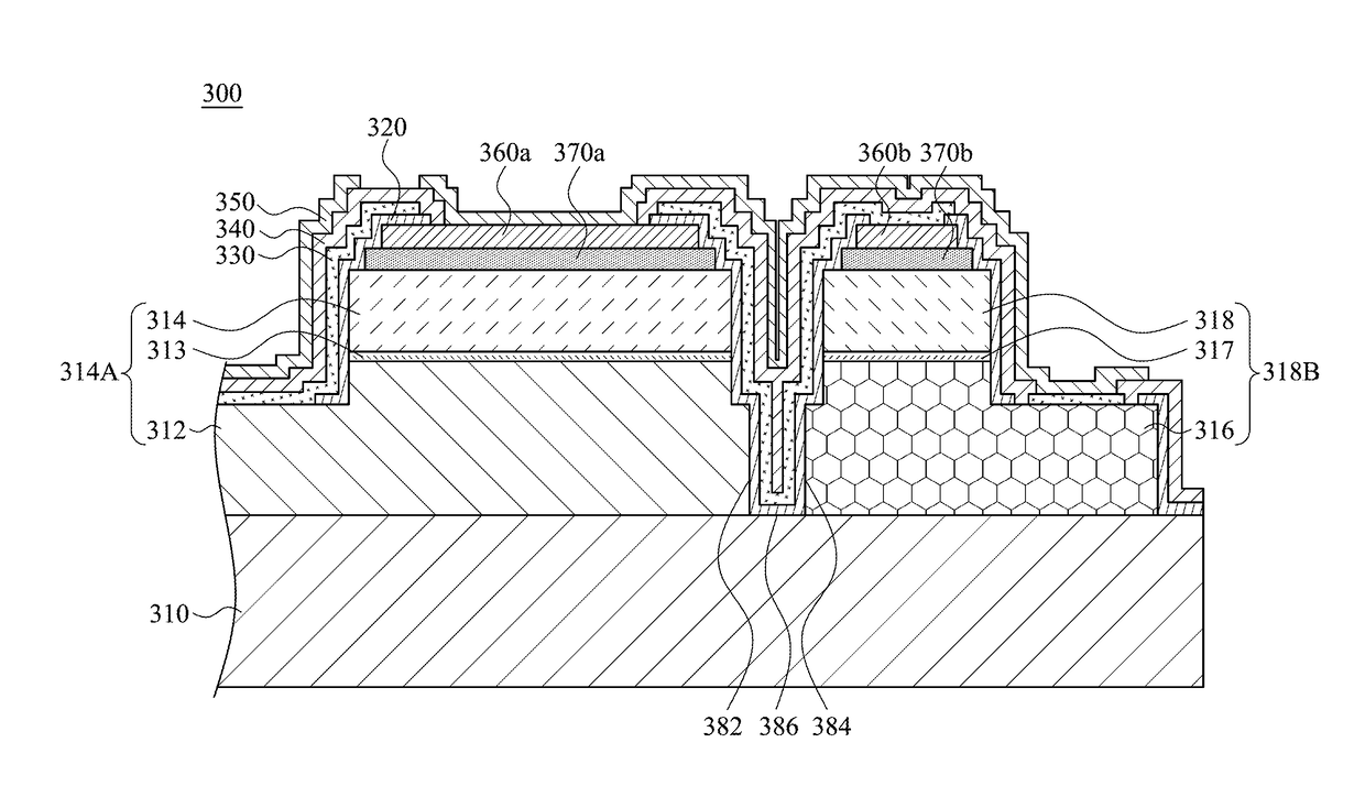
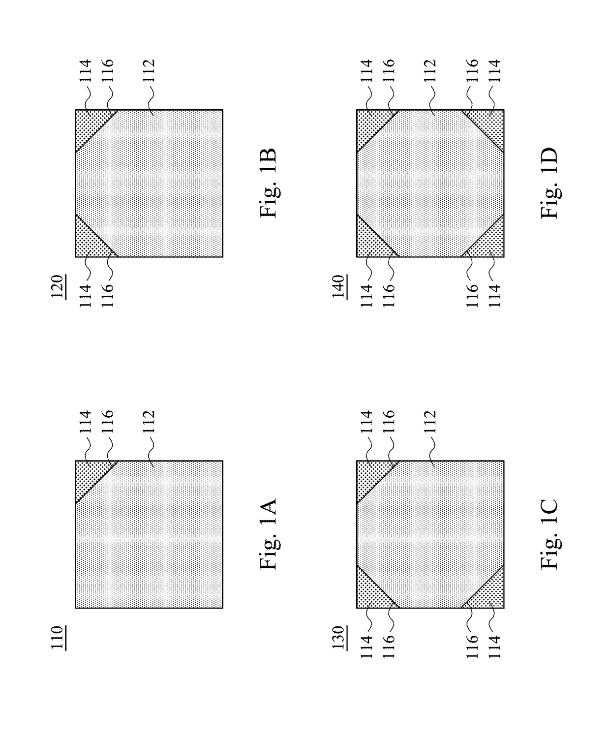
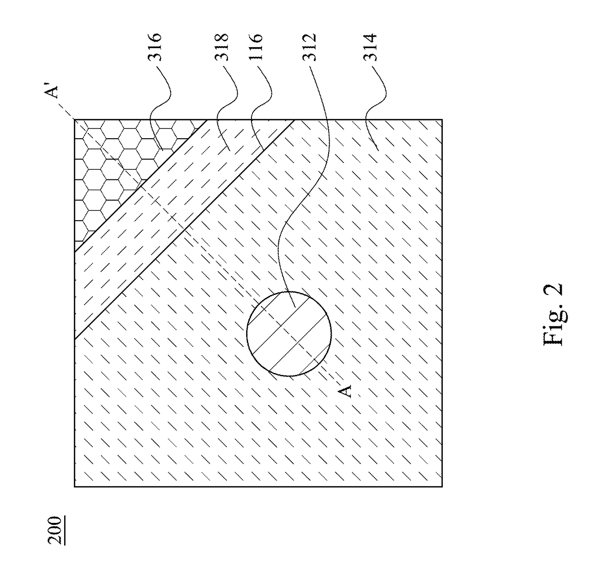
The present invention provides a light-emitting diode (LED) chip. The LED chip includes a LED structure and an electrostatic discharge (ESD) protection structure. The ESD protection structure is in a corner of the LED chip and connects with the LED structure in anti-parallel. An interface between the LED structure and the ESD protection structure is a straight line from a top view.

Description

RELATED APPLICATIONS[0001]This application claims priority to Taiwanese Application Serial Number 104144505, filed Dec. 30, 2015, which is herein incorporated by reference.BACKGROUND[0002]Field of Invention[0003]The present invention relates to a semiconductor component. More particularly, the present invention relates to a light-emitting diode chip.[0004]Description of Related Art[0005]During processes of fabricating, assembling and examining light-emitting diode chips, electrostatic charges often accumulate within the light-emitting diode chips. As the electrostatic charges accumulate to a certain extent, an electrostatic discharge would occur. Due to the high voltage, short discharge time, and large instant current of the electrostatic discharge, it would cause damage to the circuit function of the light-emitting diode chips.[0006]For preventing the damage caused by the electrostatic discharge, electrostatic discharge (ESD) protection structures are often disposed in the light-em...

Claims


Application Information

Patent Timeline
Patent Type & Authority Applications(United States)
IPC IPC(8): H01L27/02H01L29/872H01L29/866H01L33/52H01L33/62
CPCH01L27/0255H01L33/52H01L29/872H01L29/866H01L33/62H01L25/167H01L27/15H01L33/382H01L33/0008H01L33/02H01L33/44H01L2924/12041
Inventor KUO, SHIOU-YILIN, CHAO-HSIENYANG, YA-RU
Owner LEXTAR ELECTRONICS CORP
Why Eureka
Try Eureka