Liquid crystal display device and manufacturing method thereof

a technology of liquid crystal display and manufacturing method, which is applied in the direction of optics, instruments, printed circuit aspects, etc., can solve the problems of reducing the area of non-display area and the difficulty of realizing a narrow-bezel display device, and achieve the effect of reducing the area of wiring

Active Publication Date: 2017-07-20
SAMSUNG DISPLAY CO LTD
View PDF11 Cites 13 Cited by
  • Summary
  • Abstract
  • Description
  • Claims
  • Application Information

AI Technical Summary

Benefits of technology

[0008]Exemplary embodiments of the present disclosure provide a liquid crystal display (LCD) device having a narrow bezel, which is obtained by reducing the area of wiring in a non-display area.

Problems solved by technology

However, the larger the area occupied by such wiring is, the larger the area of a non-display area becomes, and the more difficult it becomes to realize a narrow-bezel display device.

Method used


Image

  • Liquid crystal display device and manufacturing method thereof
  • Liquid crystal display device and manufacturing method thereof
  • Liquid crystal display device and manufacturing method thereof

Examples


Embodiment Construction

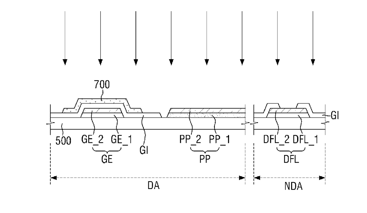
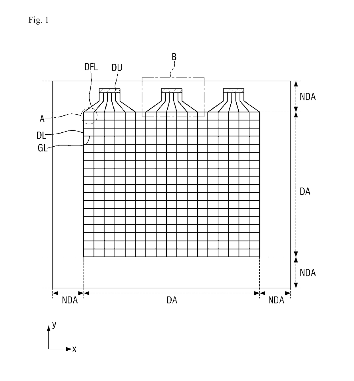
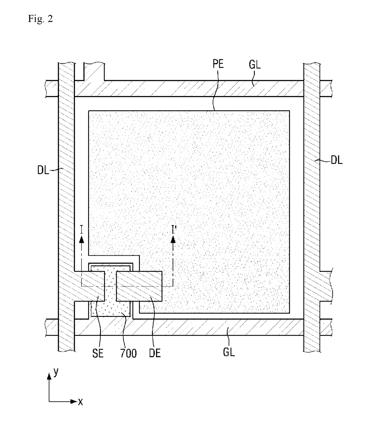
[0042]The aspects and features of the present invention and methods for achieving the aspects and features will be apparent by referring to the embodiments described herein in detail with reference to the accompanying drawings. However, the present invention is not limited to the embodiments disclosed hereinafter and may be implemented in diverse forms. The matters defined in the description, such as the detailed construction and elements, are merely provided to assist those of ordinary skill in the art in a comprehensive understanding of the invention, and the present invention is only defined within the scope of the appended claims.

The term “on” that is used to designate that an element is on another element or located on a different layer or a layer includes both a case in which an element is located directly on another element or a layer and a case in which an element is located on another element via another layer or still another element. In the entire description of the prese...


PUM

PropertyMeasurementUnit
areaaaaaaaaaaa
structureaaaaaaaaaa
semiconductoraaaaaaaaaa

Abstract

A Liquid crystal display device and manufacturing method thereof are provided. According to an exemplary embodiment of the present disclosure, an LCD device includes: a first substrate including a display area and a non-display area disposed outside of the display area; a gate electrode disposed on the first substrate and including a first-layer gate electrode and a second-layer gate electrode disposed on the first-layer gate electrode; a pixel electrode disposed on the same layer as the first-layer gate electrode; a source electrode and a drain electrode disposed on the gate electrode to be spaced from each other; and a contact connecting the drain electrode and the pixel electrode and including a first-layer contact, which is disposed on the same layer as the pixel electrode, and a second-layer contact, which is disposed on the first-layer contact.

Description

[0001]This application claims priority to Korean Patent Application No. 10-2016-0007154 filed on Jan. 20, 2016 in the Korean Intellectual Property Office, the disclosure of which is incorporated herein by reference in its entirety.BACKGROUND[0002]1. Field of the Invention[0003]The present disclosure relates to a liquid crystal display (LCD) device and a manufacturing method thereof.[0004]2. Description of the Related Art[0005]The importance of display devices has steadily grown with recent developments in multimedia technology. As a result, a variety of display devices, such as a liquid crystal display (LCD) device, an organic light-emitting diode (OLED) device, and the like, have been developed and become widespread.[0006]The LCD device, which is one of the most widely-used flat panel displays, includes two substrates on which field-generating electrodes, such as pixel electrodes and a common electrode, are formed and a liquid crystal layer interposed between the two substrates. Th...

Claims


Application Information

Patent Timeline
Patent Type & Authority Applications(United States)
IPC IPC(8): G02F1/1343G02F1/1362G02F1/1368
CPCG02F1/13439G02F1/1368G02F1/136286G02F2001/136231H01L29/7869H01L29/4908G02F2201/123G02F2202/10G02F1/1333G02F1/136227G02F1/13452H01L27/1225H01L27/124G02F1/133388G02F1/136231H05K2201/10128
Inventor LEE, KEUM HEEKIM, MAN JINKIM, YU JUNLEE, CHANG YEOLJUNG, SU JUNGJEONG, JI YOUNG
Owner SAMSUNG DISPLAY CO LTD
Why Eureka
Try Eureka