
Circuit board structure and method for manufacturing the same

Inactive Publication Date: 2017-08-10
ICHIA TECH
View PDF5 Cites 3 Cited by
  • Summary
  • Abstract
  • Description
  • Claims
  • Application Information

AI Technical Summary

Benefits of technology

This patent is about a new way to make circuit boards that solves problems with traditional methods. The method integrates the adhesive layer directly onto the circuit board, reducing production costs. Also, the pressure-sensitive gel layer is formed seamlessly on the circuit board surface, increasing adhesion strength. Overall, this new method reduces production costs and improves the quality of circuit boards.

Problems solved by technology

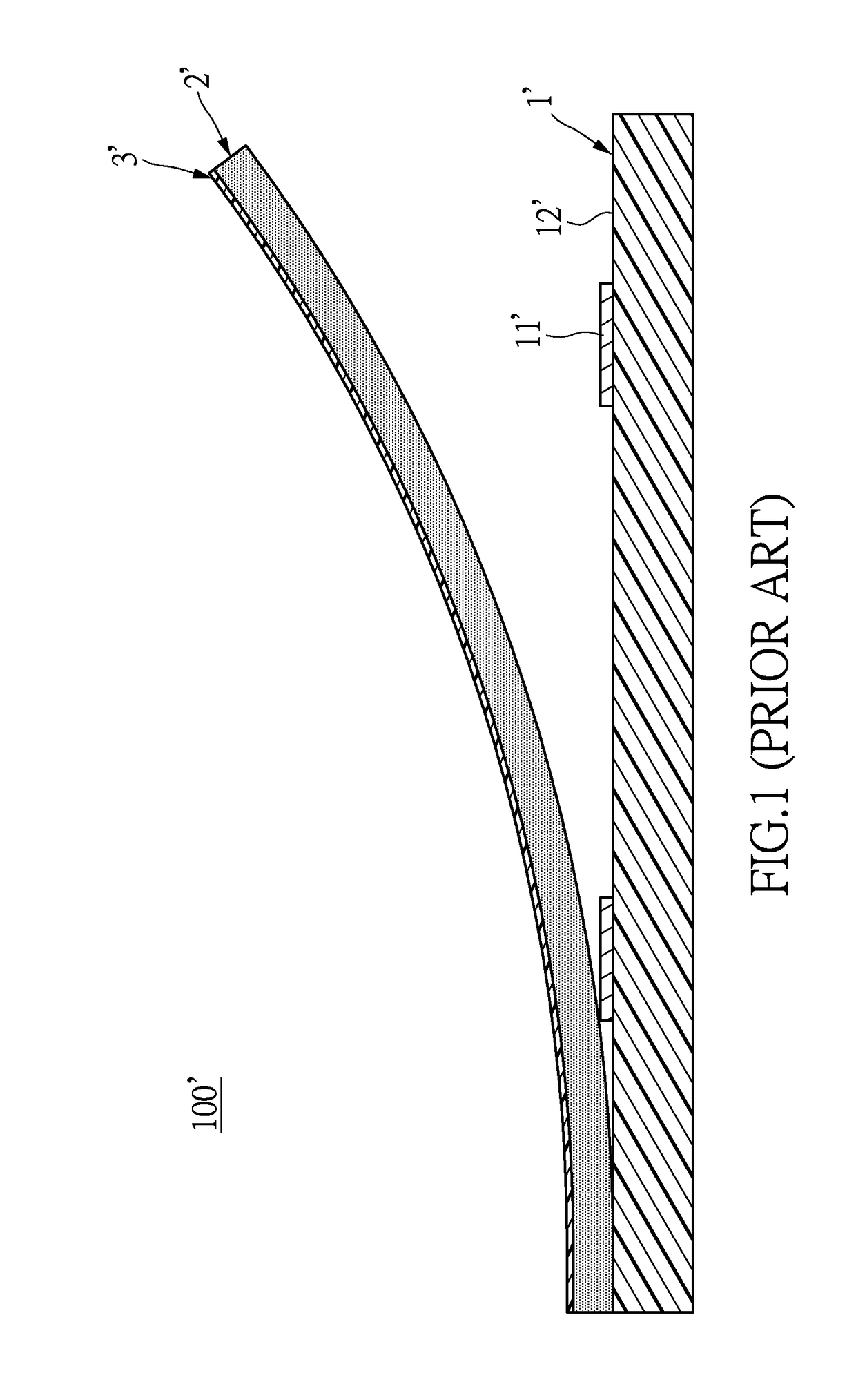
Moreover, before the double sided tape 2′ is adhered to the circuit board 1′, a larger double sided tape must be cut according to the shape of the circuit board 1′ so as to form the double sided tape 2′, but the cutting step causes material waste.

Method used


Image

  • Circuit board structure and method for manufacturing the same
  • Circuit board structure and method for manufacturing the same
  • Circuit board structure and method for manufacturing the same

Examples


first embodiment

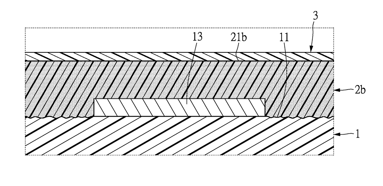
[0028]Please refer to FIGS. 4 through 8, which show a first embodiment of the instant disclosure. References are hereunder made to the detailed descriptions and appended drawings in connection with the instant invention. However, the appended drawings are merely shown for exemplary purposes, rather than being used to restrict the scope of the instant invention.

[0029]The instant disclosure provides a method for manufacturing a circuit board structure 100. The method includes steps a) to e), and the sequence of the steps of the method is disclosed for clearly understanding the instant embodiment, but the instant disclosure is not limited thereto. The steps of the method are disclosed as follows.

[0030]In step a), as shown in FIG. 4, a circuit board 1 is provided, and the circuit board 1 is preferably a flexible circuit board or a rigid-flex circuit board, but the circuit board 1 is not limited thereto. The circuit board 1 has a first board surface 11 (e.g., the top surface of the circu...

second embodiment

[0047]Please refer to FIGS. 10 through 13, which show a second embodiment of the instant disclosure. The instant embodiment is similar to the first embodiment, and the same features are not disclosed again. The main difference between the two embodiments is disclosed in the following description.

[0048]In step a), as shown in FIG. 10, a circuit board 1 is provided, and the circuit board 1 is preferably a flexible circuit board or a rigid-flex circuit board, but the circuit board 1 is not limited thereto. The circuit board 1 has a first board surface 11 and an opposite second board surface 12. The circuit board 1 has at least one conductive circuit 13 disposed on the first board surface 11. The first board surface 11 defines a predetermined portion (not labeled), and at least part of the conductive circuit 13 is disposed on the predetermined portion.

[0049]Specifically, the predetermined portion can be changed according to a designer's demand or the shape of the conductive circuit 13.

[...


PUM

PropertyMeasurementUnit
Thicknessaaaaaaaaaa
Electrical conductoraaaaaaaaaa
Sensitivityaaaaaaaaaa

Abstract

A circuit board structure includes a circuit board and an adhesive layer. The circuit board has a first board surface and an opposite second board surface, and the first board surface defines a predetermined portion. The circuit board has a conductive circuit disposed on the first board surface and at least partially arranged on the predetermined portion. The adhesive layer is seamlessly formed on the predetermined portion of the first board surface of the circuit board, and the conductive circuit arranged on the predetermined portion is seamlessly covered by the adhesive layer. A surface of the adhesive layer arranged away from the circuit board is a planar bonding surface.

Description

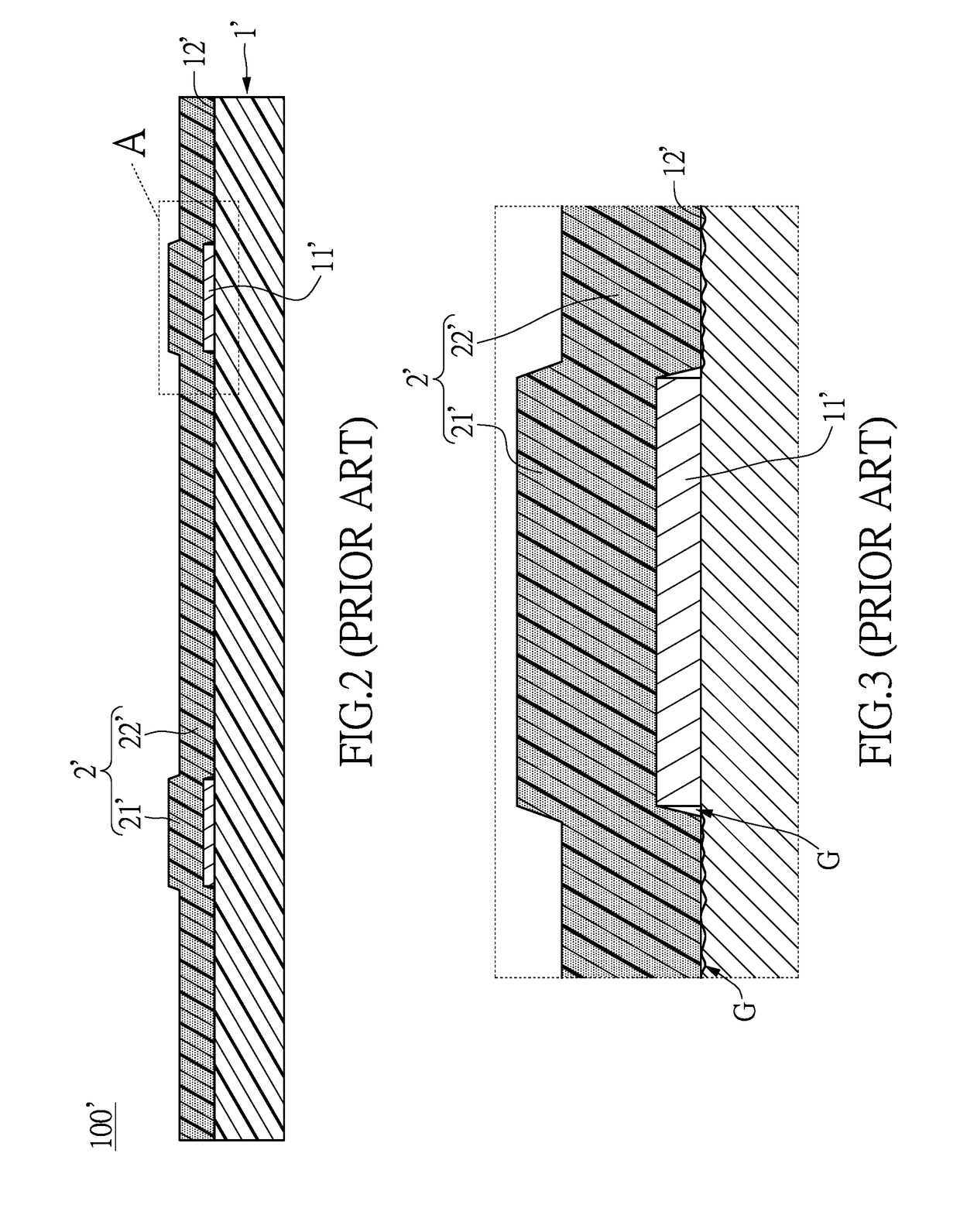
BACKGROUND OF THE INVENTION[0001]1. Field of the Invention[0002]The instant invention relates to a circuit board; in particular, to a circuit board structure and a method for manufacturing the same.[0003]2. Description of Related Art[0004]Please refer to FIGS. 1 and 2, which show a conventional circuit board structure 100′. The conventional circuit board structure 100′ is prepared by removing a release film (not shown) of a double sided tape 2′ and then adhering the double sided tape 2′ to a circuit board 1′. The double sided tape 2′ is disposed on the conductive circuit 11′ of the circuit board 1′. Accordingly, the double sided tape 2′ can be used to adhere the circuit board 1′ to a predetermined surface by removing another release film 3′.[0005]However, the circuit board 1′ and the double sided tape 2′ are manufactured respectively by two independent producing processes and are manufactured respectively by two different manufacturers, so the producing cost of the conventional circ...

Claims


Application Information

Patent Timeline
IPC IPC(8): H05K3/46H05K3/22H05K1/02
CPCH05K3/4644H05K1/0298H05K2201/0183H05K3/22H05K2203/10H05K3/4611H05K3/0058H05K3/0082H05K2201/0738H05K3/28H05K3/4635H05K3/4673C08L83/10C09J183/10H05K3/101
Inventor SUN, YUNG-HSIANGCHEN, QIN
Owner ICHIA TECH
Learn More