

Miniature wafer processing apparatus
- Summary
- Abstract
- Description
- Claims
- Application Information
AI Technical Summary
Benefits of technology
Problems solved by technology
Method used
Image

Examples
first embodiment
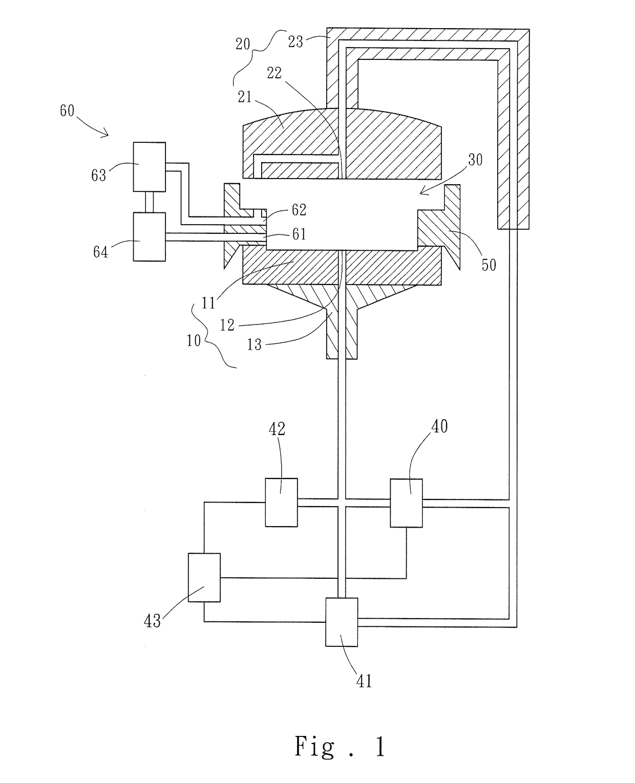
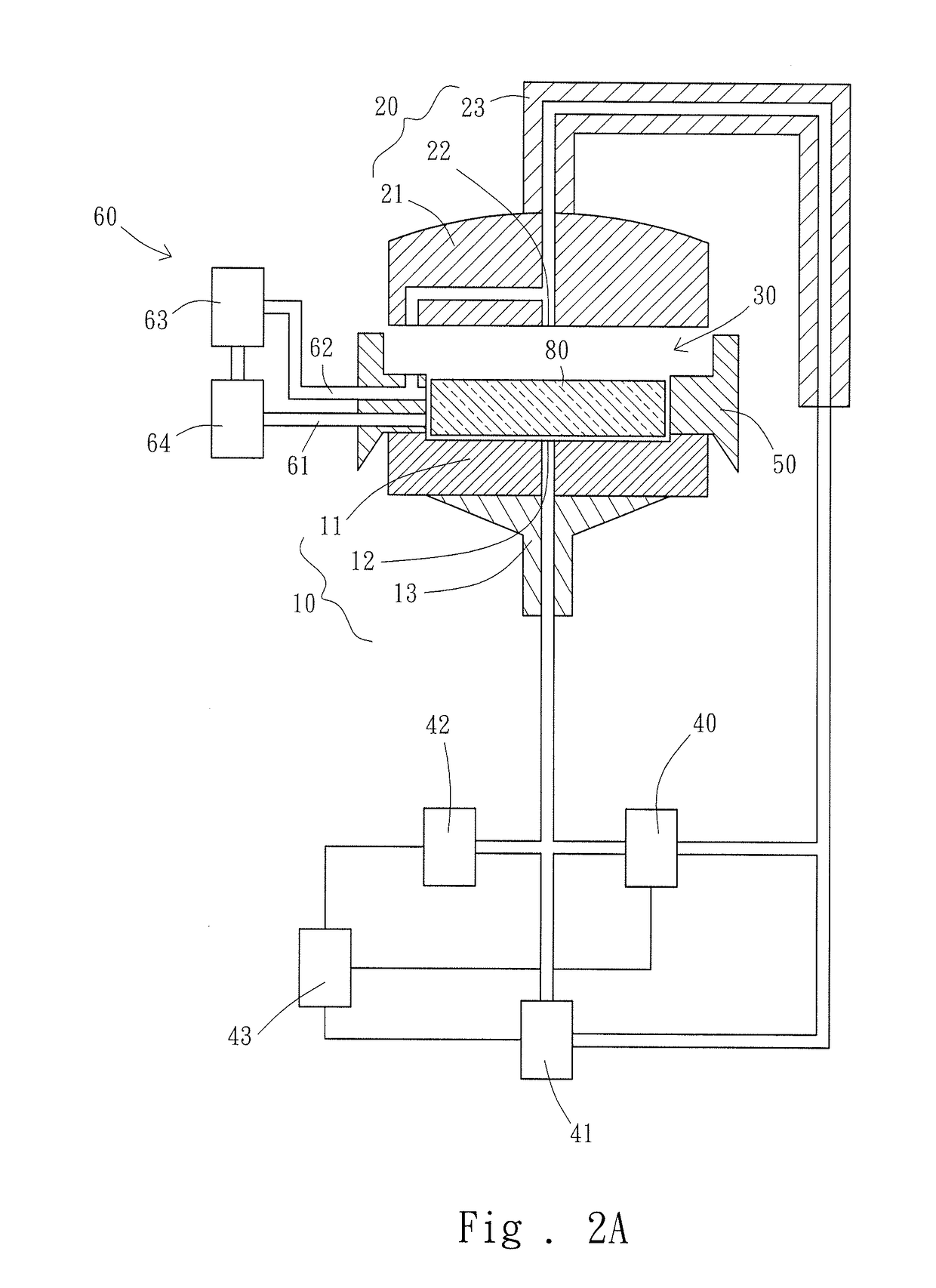
[0015]FIG. 1 and FIG. 2A to FIG. 2C are a sectional structural view and schematic diagrams of continuous operations according to the present invention. Referring to FIG. 1 and FIG. 2A to FIG. 2C, the present invention provides a miniature wafer processing apparatus that processes a wafer 80. The miniature wafer processing apparatus includes a first half portion 10, a second half portion 20 disposed above the first half portion 10, a gas supply unit 40, a liquid supply unit 41, a ring sealing member 50, and a liquid recycling member 60. The first half portion 10 includes a work platform 11, and a first hole 12 disposed on the work platform 11. The second half portion 20 includes an upper cover 21 correspondingly covering the work platform 11 to form a processing chamber 30 for accommodating the wafer 80, a second hole 22 disposed at the upper cover 21, and a lifting member 23 connected to the upper cover 21. By correspondingly covering the work platform 11 with the upper cover 21, th...
second embodiment
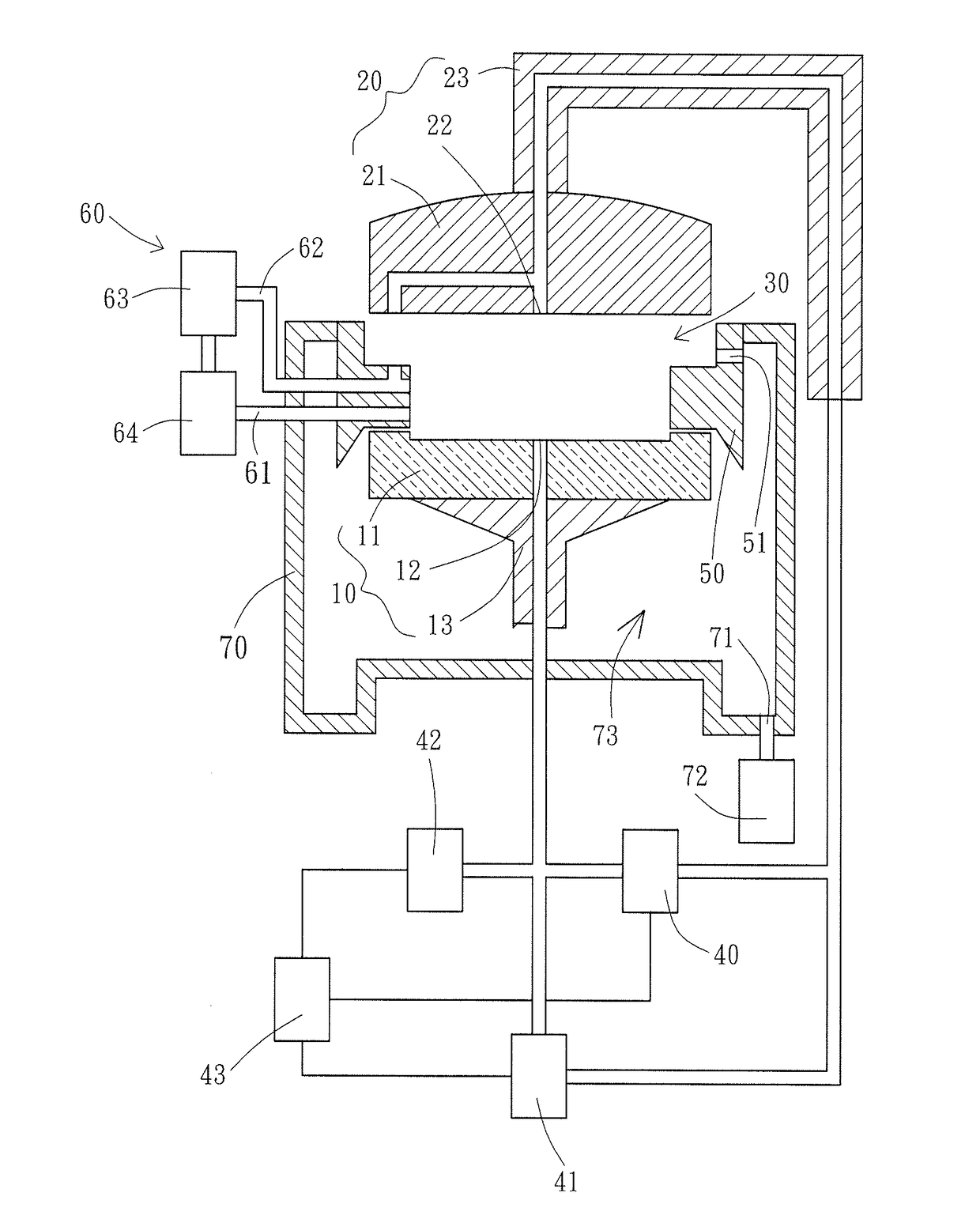
[0020]FIG. 3 and FIG. 4 are a sectional structural view and a schematic diagram illustrating a discharging mechanism according to the present invention. This embodiment further includes a gas discharging opening 51 disposed on the ring sealing member 50, and discharging member 70 disposed outside the first half portion 10 and the ring sealing member 50. When cleaning is required after the manufacturing process is complete, the lifting rotating member 13 may control the work platform 11 to descend, such that a gap between the work platform 11 and the ring sealing member 50 flows to a discharging space 73 in the discharging member 70, and the gas may be discharged from the gas discharging opening 51 to the discharging space 73 and then further discharged via a discharging opening 71 in communication with the discharging space 73. The discharging opening 71 may be connected to a negative pressure device 72 to accelerate a discharging speed of the gas and the liquid. In this embodiment,...
PUM
 Abstract
Description
Claims
Application Information