Adaptive Tuning Network for Combinable Filters

a filter network and filter technology, applied in the field of electronic circuits of radio frequency, can solve the problems of preventing selective change of band combinations, not practical for more than two or three bands, and not practical for ca radio systems

Active Publication Date: 2017-08-24
PSEMI CORP
View PDF2 Cites 29 Cited by
  • Summary
  • Abstract
  • Description
  • Claims
  • Application Information

AI Technical Summary

Benefits of technology

[0027]FIG. 11 is a block diagram of one embodiment of an RF signal switching and filter circuit that includes a multi

Problems solved by technology

Accordingly, because of the impedance mismatch, the RF signal switching and filter circuit 100 is not a practical solution for a CA radio system.
However, such an architecture prevents changing the band combinations selectively and is not practical for more than two or three bands.
However, this approach is sti

Method used


Image

  • Adaptive Tuning Network for Combinable Filters
  • Adaptive Tuning Network for Combinable Filters
  • Adaptive Tuning Network for Combinable Filters

Examples


first embodiment

[0049]A number of useful TMN 306 designs may be used in conjunction with various embodiments of the invention. As one example, FIG. 5 is a schematic diagram 500 of a tunable matching network 306. The principal adjustable impedance tuning elements are a digitally adjustable capacitor element 502 (e.g., a DTC) and a digitally adjustable inductor element 504 (e.g., a DTL) coupled in series together, and shunt connected between the IN-OUT signal path and circuit ground. In one alternative embodiment, the adjustable inductor element 504 may be replaced by a fixed inductor, and thus only the capacitor element 502 provides adjustability. In another alternative embodiment, the adjustable capacitor element 502 may be replaced by a fixed capacitor, and thus only the inductor element 504 provides adjustability. In either case, the digitally adjustable capacitor and / or inductor elements 502, 504 may be internal or external to an IC. However, in a preferred embodiment, most or all of the compone...

second embodiment

[0051]FIG. 6 is a schematic diagram 600 of a tunable matching network 306. The illustrated TMN 306 includes two digitally adjustable capacitor elements C1, C2 coupled in series between the IN-OUT signal path and circuit ground, and a digitally adjustable inductor element L coupled between circuit ground and a node between the two adjustable capacitor elements C1, C2. As in FIG. 5, one or more of the adjustable capacitor and / or inductor elements may be replaced by a fixed element, so long as at least one adjustable impedance tuning element remains. For example, the inductor element L may be fixed and all tuning accomplished using one or both of the adjustable capacitor elements C1, C2. The example circuit illustrated in FIG. 6 is particularly useful because it enables coverage of more points on a Smith chart (not just a curve), thus providing a greater range of impedance matching adjustment than some other embodiments.

third embodiment

[0052]FIG. 7 is a schematic diagram 700 of a tunable matching network 306. In the illustrated embodiment, a set of two or more LC circuits each comprising a fixed capacitor Cn and a fixed inductor Ln may be selectively connected by corresponding switches Sn to the IN-OUT signal path to set a matching impedance value for of the tunable matching network 306. Thus, adjustability is provided by selectively coupling one or more fixed-element LC circuits onto the IN-OUT signal path under the control of a TMN Control circuit 308 (as in FIG. 3) rather than utilizing digitally adjustable impedance tuning elements such as a DTC or DTL. In an alternative embodiment, the LC circuits in FIG. 7 may be replaced by a set of transmission line (TL) elements of varying impedance values that can be selectively coupled to the IN-OUT signal path under the control of the TMN Control circuit 308.

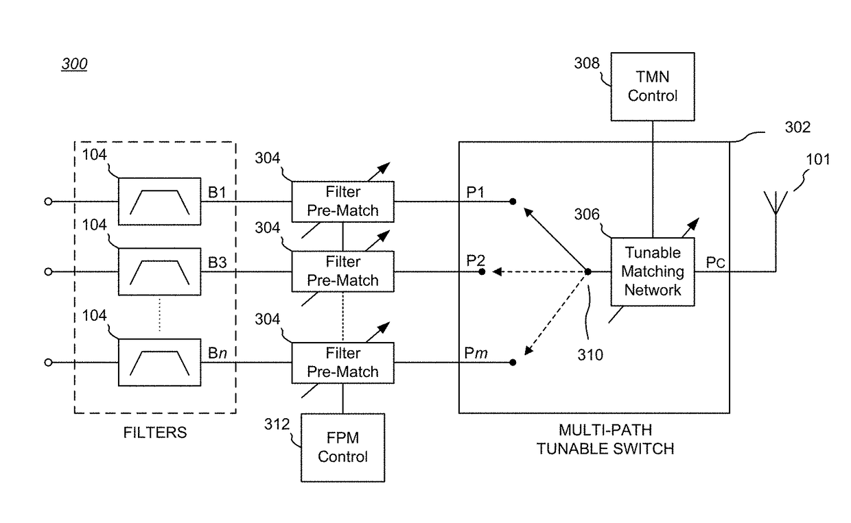
[0053]Filter Pre-Match Networks

[0054]As noted above with respect to FIG. 3, optionally, some or all RF band filt...


PUM


Abstract

A flexible multi-path RF adaptive tuning network switch architecture that counteracts impedance mismatch conditions arising from various combinations of coupled RF band filters, particularly in a Carrier Aggregation-based radio system. In one version, a digitally-controlled tunable matching network is coupled to a multi-path RF switch in order to provide adaptive impedance matching for various combinations of RF band filters. Optionally, some or all RF band filters also include an associated digitally-controlled filter pre-match network to further improve impedance matching. In a second version, some or all RF band filters coupled to a multi-path RF switch include a digitally-controlled phase matching network to provide necessary per-band impedance matching. Optionally, a digitally-controlled tunable matching network may also be included on the common port of the multi-path RF switch to provide additional impedance matching capability.

Description

BACKGROUND[0001](1) Technical Field[0002]This invention relates to electronic circuits, and more particularly to radio frequency electronic circuits and related methods.[0003](2) Background[0004]A simple radio system generally operates in one radio frequency (RF) band for transmitting RF signals and a separate RF band for receiving RF signals. An RF band typically spans a range of frequencies (e.g., 10 to 100 MHz per band), and actual signal transmission and reception may be in sub-bands of such bands, spaced apart to avoid interference. Alternatively, two widely spaced RF bands may be used for signal transmission and reception, respectively.[0005]More advanced radio systems, such as some cellular telephone systems, may be operable over multiple RF bands for signal transmission and reception, but at any one time still use only one transmit sub-band and one receive sub-band within a single RF band, or only two widely spaced transmit and receive RF bands. Such multi-band operation all...

Claims


Application Information

Patent Timeline
IPC IPC(8): H04B1/00H04B1/401H04W88/06
CPCH04B1/0067H04B1/401H04W88/06H04B1/0053H04B1/0458H03H7/40
Inventor RANTA, TERO TAPIOROBERTS, KEVINCHENG, CHIH-CHIEH
Owner PSEMI CORP
Why Eureka
Try Eureka