
Structure and method to self align via to top and bottom of tight pitch metal interconnect layers

a technology of metal interconnect layer and structure, which is applied in the direction of semiconductor devices, semiconductor/solid-state device details, electrical devices, etc., can solve the problems of degrading electrical performance, affecting the placement of the via edges relative to the interconnect layer or the line it is to contact, and becoming increasingly difficult to properly align the vias with the desired interconnect layer

Active Publication Date: 2017-09-14
INTEL CORP
View PDF12 Cites 17 Cited by
  • Summary
  • Abstract
  • Description
  • Claims
  • Application Information

AI Technical Summary

Benefits of technology

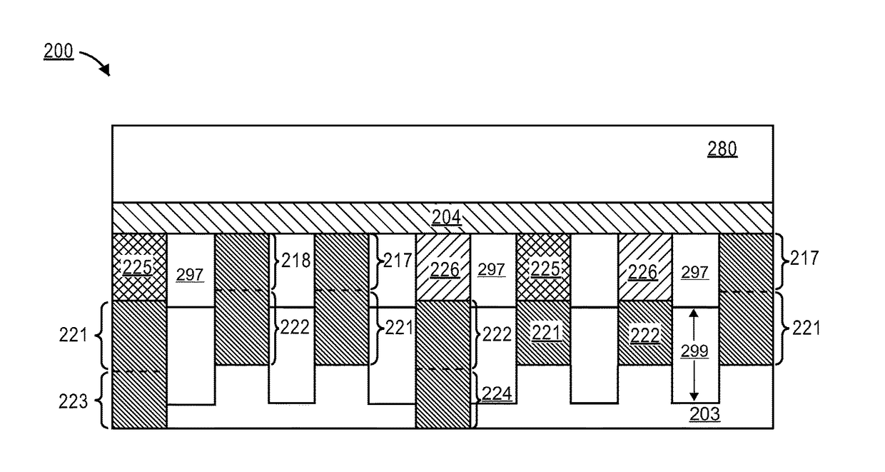
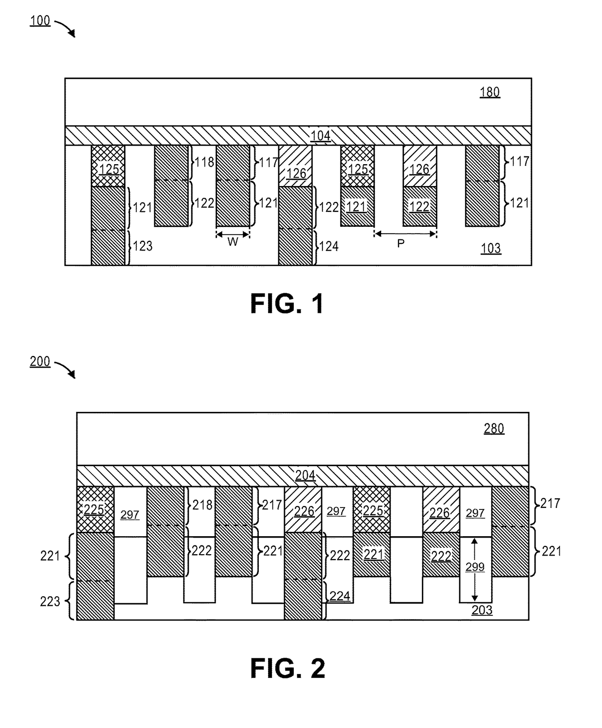
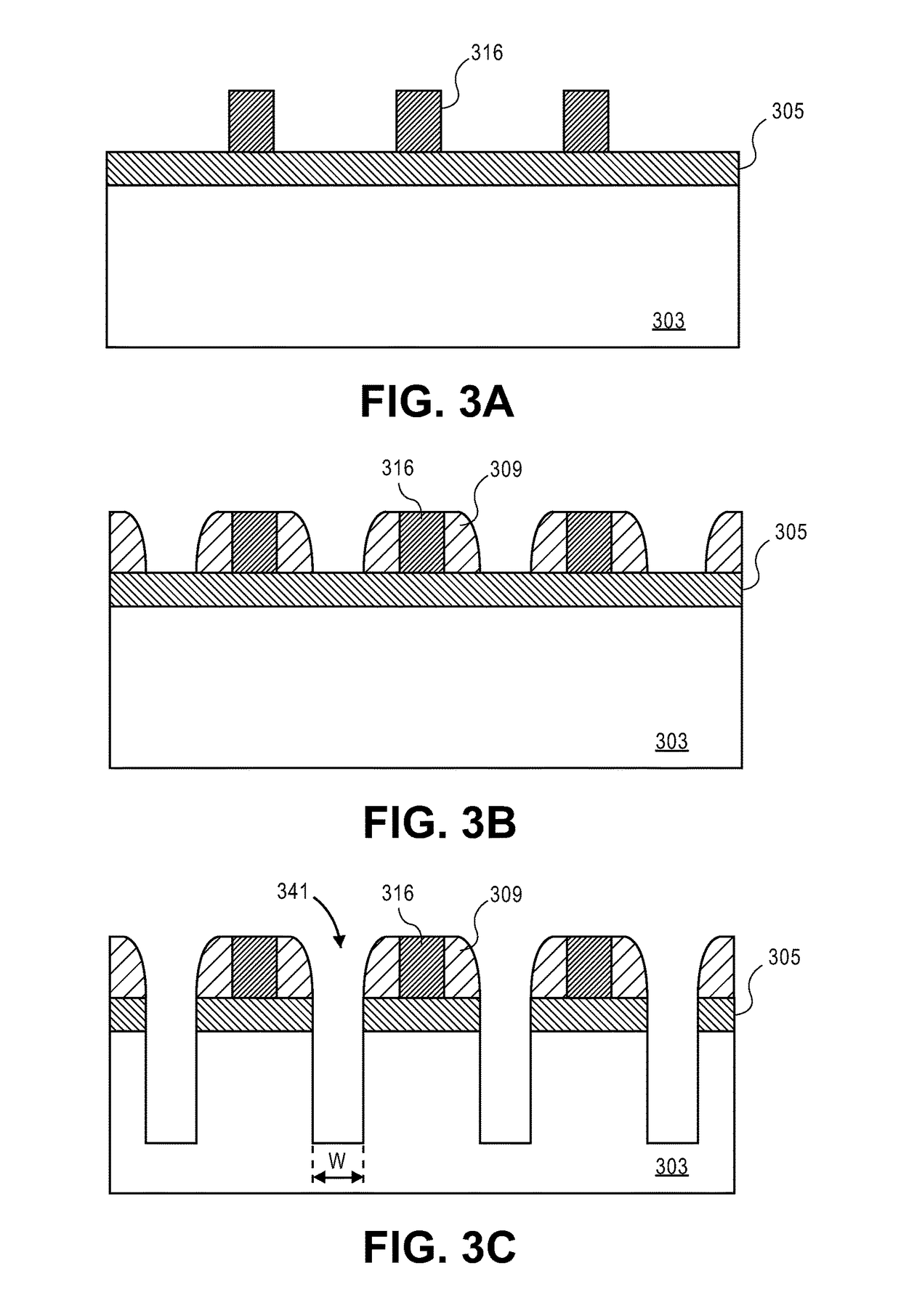
The present invention relates to interconnect structures for semiconductor devices and methods of manufacturing them. The invention addresses the difficulty of aligning vias with interconnect layers in semiconductor devices as the size of the vias becomes smaller. The invention proposes a method of forming interconnect structures with self-aligned overhead and through vias that allow for tight pitches between interconnect lines. The invention also includes methods for improving the shorting margin between an overhead via and a neighboring contact, and for forming an interposer. The technical effects of the invention include improved manufacturing efficiency and reliability of semiconductor devices.

Problems solved by technology

As these interconnect layers are manufactured with interconnect lines having smaller pitches in order to accommodate the need for smaller chips, it becomes increasingly difficult to properly align the vias with the desired interconnect layer.
In particular, during manufacturing, the location of the via edges with respect to the interconnect layer or line it is to contact may be misaligned due to natural manufacturing variation.
If the via is misaligned and contacts the wrong metal feature, the chip may short circuit resulting in degraded electrical performance.
However, reducing the via size results in an increase in resistance and reduces the yield during manufacturing.

Method used


Image

  • Structure and method to self align via to top and bottom of tight pitch metal interconnect layers
  • Structure and method to self align via to top and bottom of tight pitch metal interconnect layers
  • Structure and method to self align via to top and bottom of tight pitch metal interconnect layers

Examples


Embodiment Construction

[0011]Described herein are systems that include an interconnect structure that allows for contact formation to tightly pitched interconnect lines that include self-aligned overhead vias and self-aligned through vias and methods of forming such devices. In the following description, various aspects of the illustrative implementations will be described using terms commonly employed by those skilled in the art to convey the substance of their work to others skilled in the art. However, it will be apparent to those skilled in the art that the present invention may be practiced with only some of the described aspects. For purposes of explanation, specific numbers, materials and configurations are set forth in order to provide a thorough understanding of the illustrative implementations. However, it will be apparent to one skilled in the art that the present invention may be practiced without the specific details. In other instances, well-known features are omitted or simplified in order ...


PUM


Abstract

Embodiments of the invention include interconnect structures with overhead vias and through vias that are self-aligned with interconnect lines and methods of forming such structures. In an embodiment, an interconnect structure is formed in an interlayer dielectric (ILD). One or more first interconnect lines may be formed in the ILD. The interconnect structure may also include one or more second interconnect lines in the ILD that arranged in an alternating pattern with the first interconnect lines. Top surfaces of each of the first and second interconnect lines may be recessed below a top surface of the ILD. The interconnect structure may include a self-aligned overhead via formed over one or more of the first interconnect lines or over one or more of the second interconnect lines. In an embodiment, a top surface of the self-aligned overhead via is substantially coplanar with a top surface of the ILD.

Description

FIELD OF THE INVENTION[0001]Embodiments of the present invention relate generally to the manufacture of semiconductor devices. In particular, embodiments of the present invention relate to interconnect structures for semiconductor devices and methods for manufacturing such devices.BACKGROUND OF THE INVENTION[0002]Modern integrated circuits use conductive interconnect layers to connect individual devices on a chip and / or to send and / or receive signals external to the device. Common types of interconnect layers include copper and copper alloy interconnect lines coupled to individual devices, including other interconnect lines by interconnect through vias. It is not uncommon for an integrated circuit to have multiple levels of interconnections. For example, two or more interconnect layers may be separated from each other by dielectric materials. The dielectric layers separating interconnect levels are commonly referred to as an interlayer dielectric (ILD).[0003]As these interconnect la...

Claims


Application Information

Patent Timeline
Patent Type & Authority Applications(United States)
IPC IPC(8): H01L23/522H01L23/528H01L23/532H01L21/768
CPCH01L23/5226H01L21/76834H01L21/76808H01L21/76816H01L23/53295H01L21/76883H01L21/76897H01L23/5283H01L21/7682H01L21/0337H01L21/31144
Inventor SCHENKER, RICHARD E.CHANDHOK, MANISHBRISTOL, ROBERT L.KOBRINSKY, MAURO J.LIN, KEVIN
Owner INTEL CORP
Learn More