Thin-film bulk acoustic resonator, semiconductor apparatus comprising of such an acoustic resonator, and manufacture thereof

a technology of acoustic resonators and thin films, which is applied in the direction of electrical devices, impedence networks, and semiconductor devices. it can solve the problems of weakening the integrity of the lower and adversely affecting the performance of the fbar, and achieve the effect of improving the resonance performan

Active Publication Date: 2017-09-14
SEMICON MFG INT (SHANGHAI) CORP +1
View PDF3 Cites 15 Cited by
  • Summary
  • Abstract
  • Description
  • Claims
  • Application Information

AI Technical Summary

Benefits of technology

[0097]This summary shows that the FBAR of the present inventive concept comprises a continuous acoustic resonance film that completely separates the first and the second cavities. There is no through-hole in the acoustic resonance film, therefore the FBAR, and the semiconductor apparatus comprising of such a FBAR, can offer better resonance performance.

Problems solved by technology

The hole 105 has some undesirable effects in that it weakens the integrity of the lower electrode layer 102, the acoustic resonance film 103, and the upper electrode layer 104, adversely affecting the performance of the FBAR.

Method used


Image

  • Thin-film bulk acoustic resonator, semiconductor apparatus comprising of such an acoustic resonator, and manufacture thereof
  • Thin-film bulk acoustic resonator, semiconductor apparatus comprising of such an acoustic resonator, and manufacture thereof
  • Thin-film bulk acoustic resonator, semiconductor apparatus comprising of such an acoustic resonator, and manufacture thereof

Examples


first embodiment

A First Embodiment

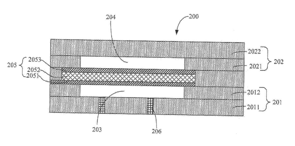
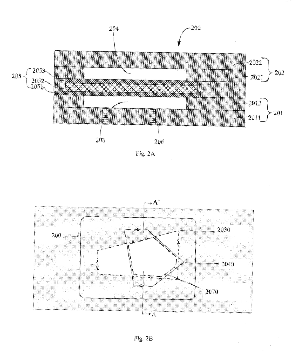
[0117]FIGS. 2A and 2B illustrate a FBAR device in accordance with one embodiment. FIG. 2A shows a schematic cross-sectional view of the FBAR device; FIG. 2B shows a top plan view of the first and the second cavities in FIG. 2A.

[0118]As illustrated in FIG. 2A, the FBAR device 200 comprises the following elements: a lower dielectric layer 201, wherein there is a first cavity 203 inside the lower dielectric layer 201. As illustrated in FIG. 2B, the top plan view of the first cavity 203 is a first polygon 2030, the first polygon 2030 has at least one pair of parallel sides, which may facilitate the measurement and control during the micro-fabrication process. The first cavity 203 may have exactly the same profiles in thickness direction.

[0119]The top plan view in FIG. 2B is obtained by observing the corresponding element in the schematic diagram of FIG. 2A looking down from the “top” of FIG. 2A. In this application, the “top plan view” of an element in a schematic diag...

second embodiment

A Second Embodiment

[0143]FIGS. 3N1 and 3P depict another embodiment of the semiconductor apparatus in accordance with this inventive concept.

[0144]Referring to FIG. 3N1, as an example, the semiconductor apparatus in the inventive concept may comprise an isolation trench layer 302 and a first dielectric layer 303 on the isolation trench layer 302. The isolation trench layer 302 may be filled with a filling material such as silicon-based oxide, nitride, or oxynitride.

[0145]The first dielectric layer 303 may be made of materials such as silicon-based oxide or nitride. For example, it may be made of silicon dioxide (SiO2), carbon-fluorine compound (CF), carbon-doped silicon oxide (SiOC), silicon nitride (SiN), or silicon carbonitride (SiCN). Alternatively, the first dielectric layer 303 may also be made of carbon-fluorine compounds comprising of carbonitride (SiCN) film. The major components of the carbon-fluorine compound are fluorine (F) and carbon (C). The carbon-fluorine compounds m...

third embodiment

A Third Embodiment

[0207]Referring to FIGS. 3A, 3B, 3C, 3D, 3E, 3F1, 3F2, 3G, 3H, 3I, 3J, 3K, 3L1, 3L2, 3M, 3N1, 3N2, 3N3, 3O, and 3P, one embodiment of a manufacturing method for a semiconductor apparatus of the inventive concept is described. FIGS. 3A, 3B, 3C, 3D, 3E, 3F1, 3G, 3H, 3I, 3J, 3K, 3L1, 3M, 3N1, 3O, and 3P show the cross-sectional views that illustrate the elements and / or structures formed in accordance with one or more embodiments of the manufacturing method. FIGS. 3F2, 3L2, 3N2, and 3N3 show the top plan view of the first or the second cavity.

[0208]Referring to FIG. 3A, a base substrate 300 is provided, and an isolation trench layer 302 is formed on the base substrate 300. A first dielectric layer 303 is formed above the substrate 300 such that it covers the isolation trench layer 302. A first metal connecting layer 3051 is formed on the first dielectric layer 303.

[0209]The base substrate 300 may be a silicon-based substrate, it may be made of silicon (Si), germanium (...


PUM

PropertyMeasurementUnit
shapeaaaaaaaaaa
dielectricaaaaaaaaaa
piezoelectricaaaaaaaaaa

Abstract

A thin-film bulk acoustic resonator, a semiconductor apparatus including the acoustic resonator and its manufacturing methods are presented. The thin-film bulk acoustic resonator includes a lower dielectric layer, a first cavity inside the lower dielectric layer, an upper dielectric layer, a second cavity inside the upper dielectric layer, and a piezoelectric film that is located between the first and the second cavities and continuously separates these two cavities. The plan views of the first and the second cavities have an overlapped region, which is a polygon that does not have any parallel sides. The piezoelectric film in this inventive concept is a continuous film without any through-hole in it, therefore it can offer improved acoustic resonance performance.

Description

CROSS-REFERENCE TO RELATED APPLICATION[0001]This application claims priority to and benefit of Chinese Patent Application No. 201610135996.6 filed on Mar. 10, 2016, which is incorporated herein by reference in its entirety.BACKGROUND[0002](a) Field of the Invention[0003]The present inventive concept relates to a film bulk acoustic resonator, a semiconductor apparatus including the film bulk acoustic resonator, and manufacturing methods thereof.[0004](b) Description of the Related Art[0005]Thin-film Bulk Acoustic Resonator (FBAR) is a micro-electro-mechanical (MEMS) based radio frequency (RF) device that has been widely used in wireless devices such as cell phone. FBAR device offers high signal sensitivity, wide frequency response spectrum, and good output linearity. It also has a small footprint and can be integrated into existing complementary metal-oxide-semiconductor (CMOS) fabrication process.[0006]FIG. 1 depicts an example of a conventional FBAR. In manufacturing the structure ...

Claims


Application Information

Patent Timeline
Patent Type & Authority Applications(United States)
IPC IPC(8): H03H9/17H01L27/20H03H3/02H03H9/02H03H3/007
CPCH03H9/171H03H9/02007H03H3/0073H03H2003/027H01L27/20H03H2009/155H03H3/02H03H9/174H03H2003/023H03H9/0547H03H9/173H03H9/587H03H2003/021Y10T29/49005Y10T29/42H03H9/1035H10N39/00
Inventor HUANG, HERB HEDROWLEY, CLIFFORD IANZHU, JIGUANGLI, HAITING
Owner SEMICON MFG INT (SHANGHAI) CORP
Why Eureka
Try Eureka