Light emitting element, light emitting device, and electronic apparatus

a light emitting device and light emitting element technology, applied in the direction of diodes, semiconductor devices, electrical devices, etc., can solve the problems of deterioration of light emission characteristics, damage to second electrodes, and generation of concavities and convexities, and achieve superior display quality and reliability quality.

Active Publication Date: 2017-09-28
SEIKO EPSON CORP
View PDF0 Cites 9 Cited by
  • Summary
  • Abstract
  • Description
  • Claims
  • Application Information

AI Technical Summary

Benefits of technology

[0029]According to the configuration of the application example, it is possible to provide the electronic apparatus that has superior display quality and reliability quality.

Problems solved by technology

Meanwhile, when the second electrode that has Ag as a main component is used, there is a concern that concavities and convexities are generated in the second electrode due to aggregation of Ag atoms, and the second electrode is damaged due to stress being applied to the concavities and convexities according to a load from an inorganic compound film that is formed on an upper layer.
That is, when content of Ag contained in the second electrode is high in order to improve brightness of the organic EL element, there is a problem in that there is a concern that influence tends to be received due to reaction of Ag with moisture or oxygen and leads to deterioration of a light emission characteristic and reliability quality reduction in light emission life.
Although it is possible to improve brightness of the light emitting element as the amount of Ag contained in the second electrode is great, power supply performance deteriorates due to film quality being reduced when content of Ag is too great.

Method used


Image

  • Light emitting element, light emitting device, and electronic apparatus
  • Light emitting element, light emitting device, and electronic apparatus
  • Light emitting element, light emitting device, and electronic apparatus

Examples


first embodiment

Light Emitting Device

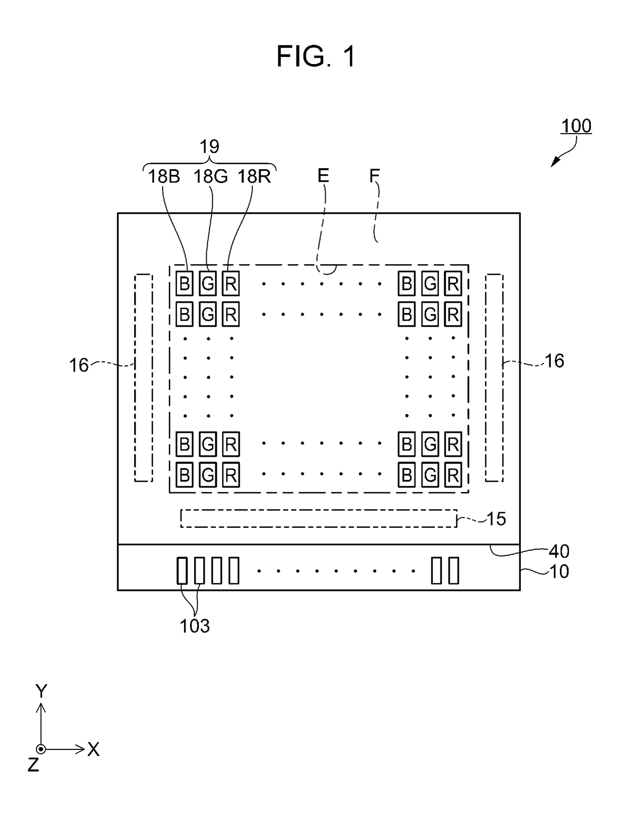
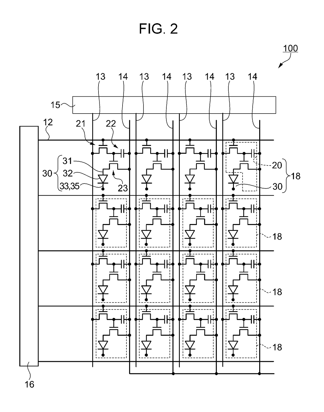
[0043]First, an organic EL apparatus is described with reference to FIGS. 1 to 3 as a light emitting device according to a first embodiment. FIG. 1 is a schematic planar view illustrating a configuration of the organic EL apparatus according to the first embodiment. FIG. 2 is a equivalent circuit schematic illustrating an electrical configuration of the organic EL apparatus according to the first embodiment. FIG. 3 is a schematic planar view illustrating an arrangement of organic EL elements in sub pixels. An organic EL apparatus 100 according to the embodiment is a suitable self-luminous micro display in a display portion of a head mounted display (HMD) described above.

Light Emitting Device Structure

[0044]As shown in FIG. 1, the organic EL apparatus 100 as the light emitting device according to the embodiment has an element substrate 10 and a protective substrate 40. Both substrates are adhered disposed opposite a filler 42 (refer to FIG. 4).

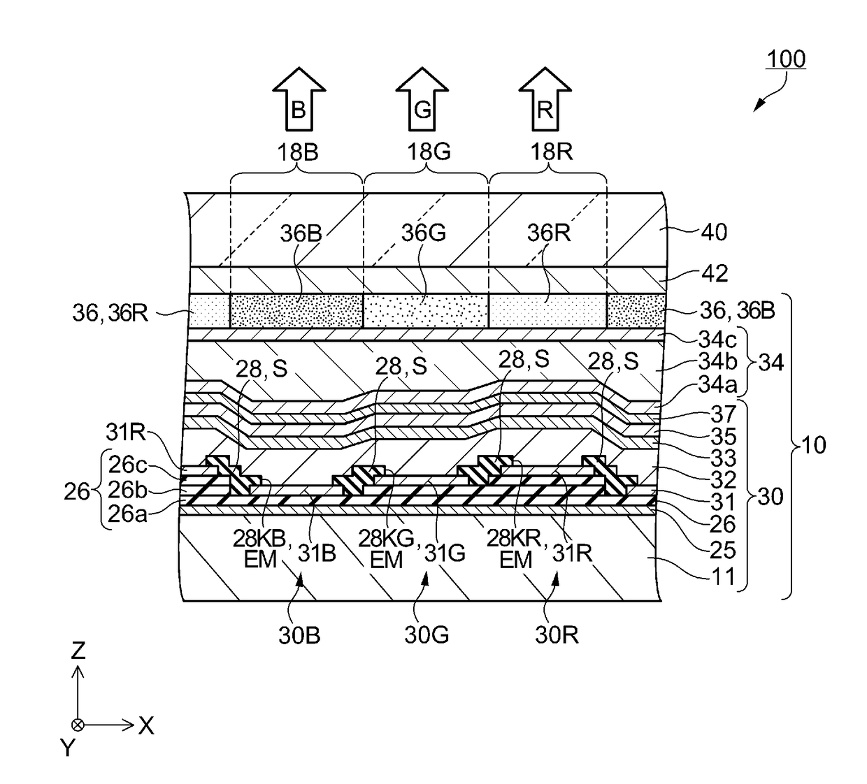
[0045]The element s...

second embodiment

Electronic Apparatus

[0138]Next, an electronic apparatus according to a second embodiment will be described with reference to FIG. 9. FIG. 9 is a schematic view illustrating a configuration of a head mounted display as an electronic apparatus according to the second embodiment.

[0139]As shown in FIG. 9, a head mounted display (HMD) 1000 according to the second embodiment is provided with two display portions 1001 which are provided to correspond to left and right eyes. An observer M is able to see characters, images, and the like which are displayed on the display portions 1001 by mounting the head mounted display 1000 on their head as glasses. For example, if an image is displayed taking into account a parallax in the left and right display portions 1001, it is also possible to enjoy viewing three-dimensional moving images.

[0140]The organic EL apparatus 100 according to the first embodiment is mounted on the display portions 1001. Accordingly, it is possible to provide a small light ...

modification example 1

[0144]In the first embodiment, the material of the adsorption layer 37 that is provided with the organic EL element 30 is Mg, but the invention is not limited to the aspect. The material of the adsorption layer 37 (reductive material that reduces the material of the electron injection layer 33) may be a metal other than Al. Al is superior in reduction of an Li compound, treatment during manufacture is comparatively easy, and it is possible to easily use a vapor deposition method such as deposition. In addition, the material of the adsorption layer 37 may be an organic material. In a case where the organic material is used in the material of the adsorption layer 37, it is preferable that the absorption coefficient of light is small, and there is the organic material that has a water-absorbing property. Note that, in a case where the organic material is used in the material of the adsorption layer 37, when the lower value of the thickness of the adsorption layer 37 is set, it may be c...


PUM


Abstract

An organic EL element includes a pixel electrode, a light emitting function layer that is formed on the pixel electrode, an electron injection layer formed on the light emitting function layer, and a counter electrode that is formed on the electron injection layer and that has semi-transmissive reflectivity, in which the counter electrode contains a reductive material that reduces material of the electron injection layer and Ag with atomic ratio of 75% or more, and an adsorption layer is formed on the counter electrode.

Description

BACKGROUND[0001]1. Technical Field[0002]The present invention relates to a light emitting element, a light emitting device, and an electronic apparatus.[0003]2. Related Art[0004]Since it is possible for an organic EL element as a light emitting element to be miniaturized or thinned in comparison to a light emitting diode (LED), application has been observed of a micro display such as a head mounted display (HMD) or an electronic view finder (EVF). In such a micro display, in order to improve brightness, a configuration is suggested in which a main component of an electrode (second electrode) on a side to which light is extracted is Ag (for example, refer to Japanese Patent No. 5411469).[0005]Meanwhile, when the second electrode that has Ag as a main component is used, there is a concern that concavities and convexities are generated in the second electrode due to aggregation of Ag atoms, and the second electrode is damaged due to stress being applied to the concavities and convexiti...

Claims


Application Information

Patent Timeline
Patent Type & Authority Applications(United States)
IPC IPC(8): H01L51/52H01L27/32
CPCH01L51/5203H01L51/5253H01L51/5259H01L27/322H01L27/3211H10K50/82H10K50/844H10K59/38H10K50/826H10K50/852H10K2102/351H01L33/36H01L33/40H01L33/42H10K50/824H10K30/865H10K50/00H10K50/17H10K50/81H10K50/156H10K50/166H10K50/167H10K50/171H10K50/805H10K50/814H10K50/828H10K50/846H10K59/00H10K59/35
Inventor SHIRATORI, KOYAHANAMURA, YUKIASAKAWA, TSUTOMU
Owner SEIKO EPSON CORP
Why Eureka
Try Eureka