Electronic device, method of manufacturing the same, and camera
- Summary
- Abstract
- Description
- Claims
- Application Information
AI Technical Summary
Benefits of technology
Problems solved by technology
Method used
Image

Examples
first embodiment
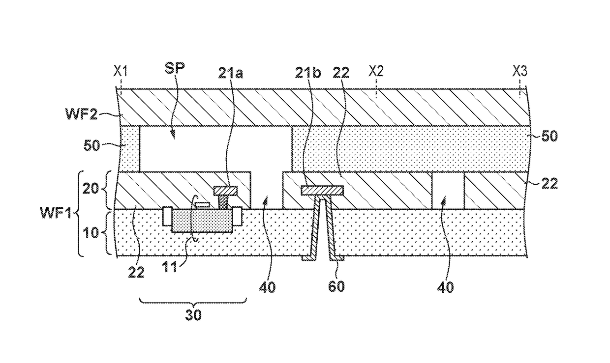
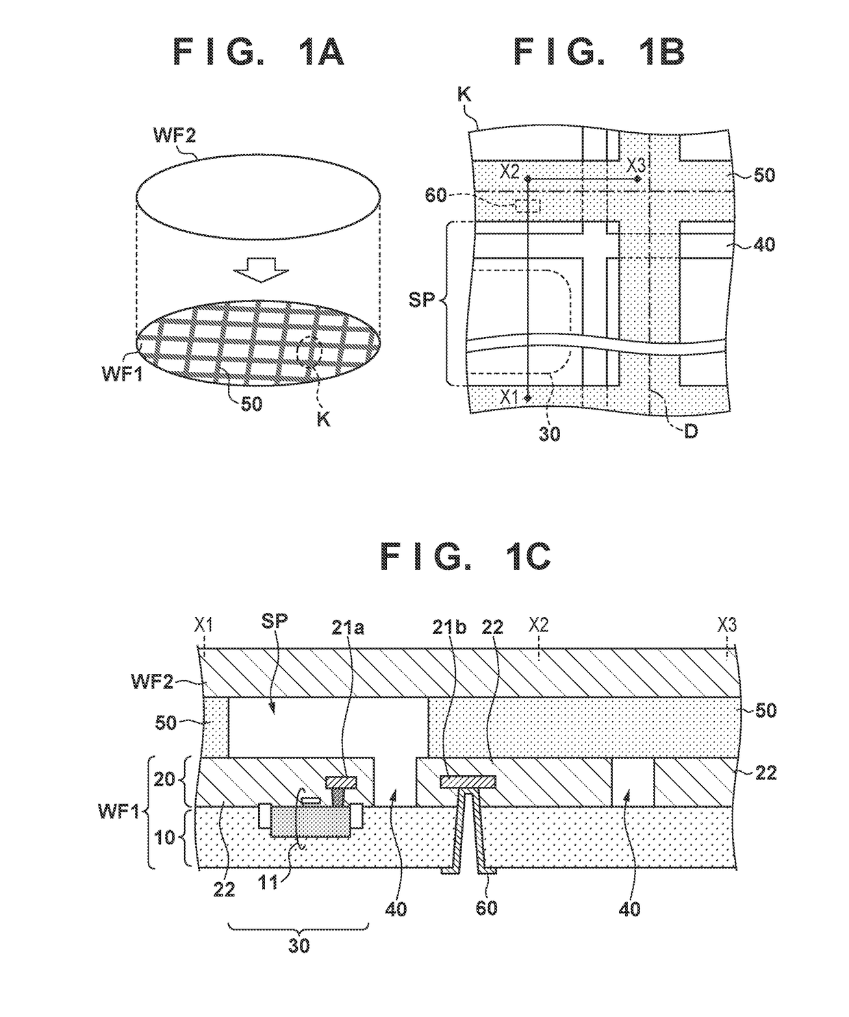
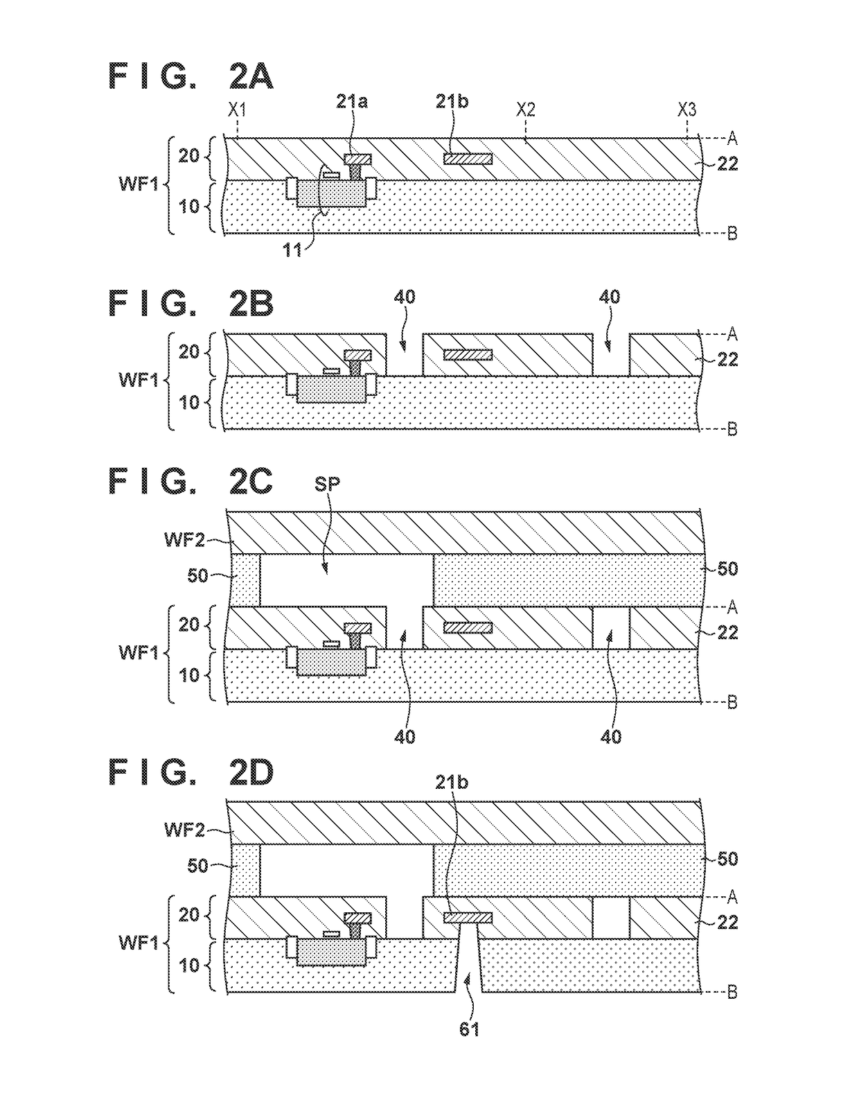
[0016]A method of manufacturing an electronic device according to the first embodiment will be described with reference to FIGS. 1A, 1B, 1C, 2A, 2B, 2C, and 2D. FIG. 1A shows one step in the method of manufacturing an electronic device in WLCSP (Wafer Level Chip Size Package). More specifically, FIG. 1A shows a step of adhering a second wafer WF2 to a first wafer WF1 as indicated by the arrow in FIG. 1A. A grid-shaped surrounding member 50 is formed on the upper surface (the surface on the adhering side) of the first wafer WF1. The wafers WF1 and WF2 are fixed to each other via the surrounding member 50. Note that when adhering the first wafer WF1 and the second wafer WF2, the surrounding member 50 may be formed on the side of the second wafer WF2. The wafers WF1 and WF2 fixed to each other undergo a process of forming an external electrode (to be described later) and then dicing, whereby one or more electronic devices are obtained. In the electronic device, the first wafer WF1 afte...
second embodiment
[0043]FIG. 3A is an enlarged view of a region K of a first wafer WF1 according to the second embodiment. FIG. 3B is a schematic view of the sectional structure taken along a cut line X1-X2-X3 in FIG. 3A. This embodiment is different from the above-described first embodiment in that at the intersection between a trench 40 and a surrounding member 50, a cover member 70 is arranged between the trench 40 and the surrounding member 50 so as to separate them and prevent the trench 40 from being filled with the surrounding member 50. That is, at the intersection between the trench 40 and the surrounding member 50, the cover member 70 is arranged on an insulating member 22 so as to be laid across the trench 40, thereby preventing the trench 40 from being filled with the surrounding member 50 to be formed later. According to this embodiment, the trench 40 is not filled with the surrounding member 50 at the intersection with respect to the surrounding member 50 in a planar view. Hence, this e...
third embodiment
[0048]FIG. 6A is an enlarged view of a region K of a first wafer WF1 according to the third embodiment. FIG. 6B is a schematic view of the sectional structure taken along a cut line X4-X5.
[0049]First, this embodiment is different from the above-described embodiments in that a wiring structure 20 further includes a guard ring 80 included in an insulating member 22. More specifically, the guard ring 80 can be formed to surround a region 30 in a planar view, and can include a wiring pattern, a contact plug, and a via hole, like a conductive member 21. The guard ring 80 has a function of preventing water or humidity from the trench 40 from entering the inside of the wiring structure 20. Note that in this example, a case in which the number of wiring layers is 3 is shown. However, the number of wiring layers is not limited to that of this example.
[0050]Second, this embodiment is different from the above-described embodiments in that a passivation film 23 is formed as the uppermost layer ...
PUM
 Abstract
Description
Claims
Application Information
 - R&D Engineer
- R&D Manager
- IP Professional
- Industry Leading Data Capabilities
- Powerful AI technology
- Patent DNA Extraction
Browse by: Latest US Patents, China's latest patents, Technical Efficacy Thesaurus, Application Domain, Technology Topic.
© 2024 PatSnap. All rights reserved.Legal|Privacy policy|Modern Slavery Act Transparency Statement|Sitemap