Method for manufacturing organic el display panel

a technology of electroluminescence and display panels, applied in the direction of printing, electrical equipment, semiconductor devices, etc., can solve the problems of inability to correct and defect the nozzle, and achieve the effects of reducing manufacturing efficiency, and reducing ink application amoun

Active Publication Date: 2017-10-19
JOLED INC
View PDF0 Cites 8 Cited by
  • Summary
  • Abstract
  • Description
  • Claims
  • Application Information

AI Technical Summary

Benefits of technology

[0012]According to the method for manufacturing an organic EL display panel pertaining to the aspect above, even if a defective nozzle occurs among the nozzles, a decrease in ink application amount can be supplemented by changing a reserve nozzle to a use-nozzle. In other words, according to the manufacturing method, a decrease in ink application amount due to occurrence of a defective nozzle can be supplemented by a method that is simple and suppresses a decrease in manufacturing efficiency.

Problems solved by technology

Among this large number of nozzles, adhesion of dried ink or foreign matter may generate defective nozzles for which ink application location or application amount deviates greatly from set values and for which correction is impossible.

Method used


Image

  • Method for manufacturing organic el display panel
  • Method for manufacturing organic el display panel
  • Method for manufacturing organic el display panel

Examples


embodiment

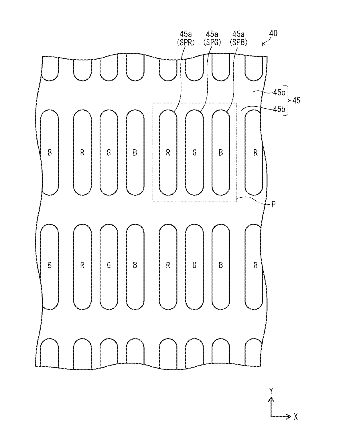
[0062]The following describes a method for manufacturing an organic EL display panel pertaining to one aspect of the present invention, with reference to the drawings. Note that the drawings are schematic, and dimensions, vertical to horizontal ratios, etc., may differ from actual implementation. Further, in the present application, plan view diagrams and plan view photographs are diagrams and photographs of objects viewed from vertically above, and in the case of the organic EL display panel, the diagrams and photographs are from a view vertically above a substrate top surface. Further, a planar shape refers to a shape appearing in a plan view diagram or plan view photograph.

1. Overall Configuration of Organic EL Display Device 1

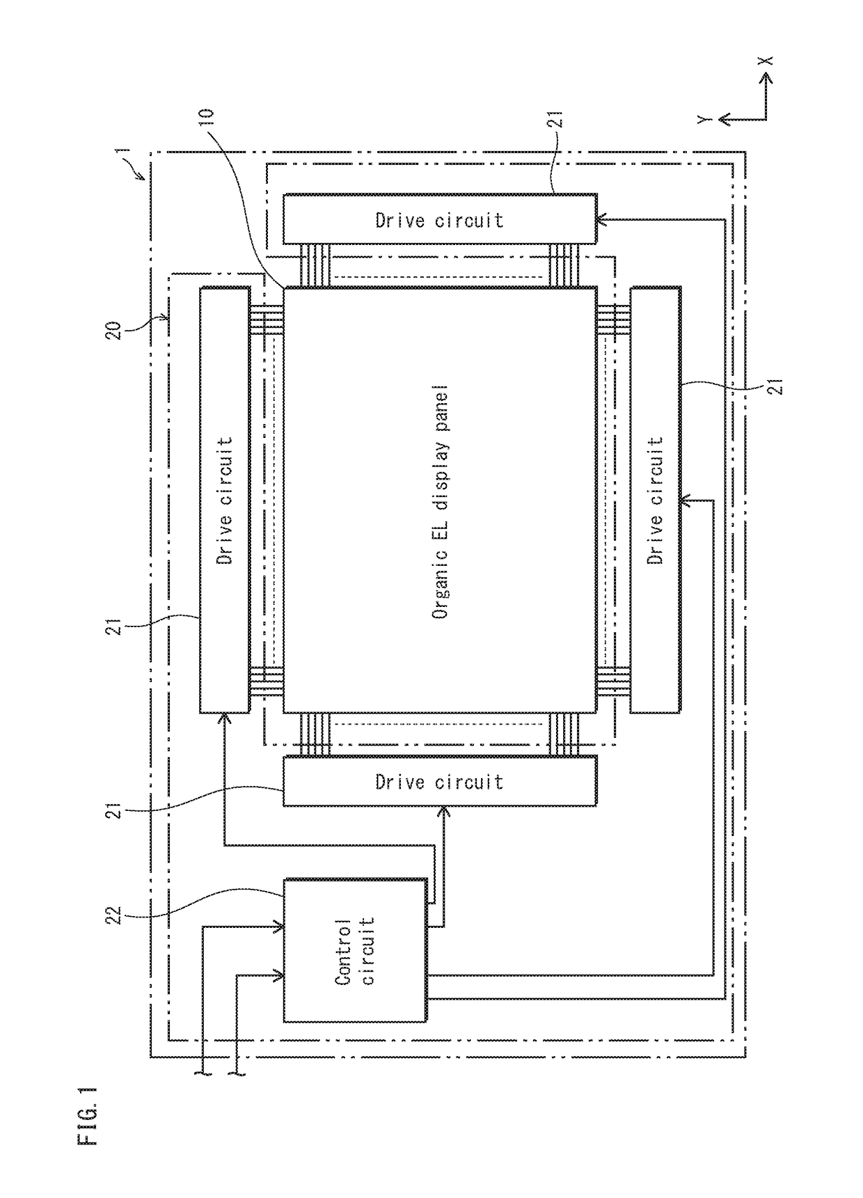
[0063]FIG. 1 is a block diagram showing an overall configuration of an organic EL display device 1. The organic EL display device 1 is a display device used, for example, in televisions, personal computers, portable terminals, and commercial displays (elect...


PUM


Abstract

Forming functional layers including functional material in application regions by applying ink to the application regions then drying the ink, which contains the functional material, by causing nozzles to be scanned relative to the substrate along the row direction while, among the nozzles, only use-nozzles that are not selected as a defective nozzle eject the ink, the nozzles being arranged in the column direction over the substrate and including a nozzle selected in advance as a defective nozzle. Among the nozzles, when applying the ink, at least one reserve nozzle is present, a reserve nozzle being a nozzle that is not one of the use-nozzles, is not selected as the defective nozzle, passes over the application region, and does not eject the ink.

Description

TECHNICAL FIELD[0001]The present invention relates to methods for manufacturing organic electroluminescence (EL) display panels in which organic EL elements are arranged, and in particular to methods for manufacturing organic EL display panels by using inkjet methods.BACKGROUND ART[0002]In an organic EL display panel in which organic EL elements are arranged in a matrix on a substrate, light emitted from organic EL elements is used as pixels to display an image.[0003]An organic EL element has a structure in which a functional layer including a functional material, for example an organic light-emitting layer including an organic light-emitting material, is sandwiched between a pair of electrodes. Aside from an organic light-emitting layer, a functional layer may be a hole or electron injection layer, a hole or electron transport layer, a hole or electron blocking layer, a buffer layer, etc., the function of which may be determined by a functional material contained within and by a re...

Claims


Application Information

Patent Timeline
Patent Type & Authority Applications(United States)
IPC IPC(8): H01L27/32H01L51/00B41J2/045H01L51/56H01L51/52
CPCH01L27/3246H01L51/56H01L51/0005H01L27/3211H01L2227/323B41J2/04586H01L51/5206H01L51/5221H01L51/0021B41J2/0451B41J2/2139B41J2/51H10K59/122H10K59/35H10K71/00H10K71/135H10K50/81H10K50/82H10K59/1201H10K71/60
Inventor GOTO, MASASHINAGUMO, TAKAOMIYOSHI, TAKAYUKI
Owner JOLED INC
Why Eureka
Try Eureka