Amplification circuit

a technology of amplification circuit and amplification circuit, which is applied in the direction of low-noise amplifiers, gated amplifiers, amplifiers using switched capacitors, etc., can solve the problems of increasing the difference in pass loss, difficult to use the circuit as a reception circuit that handles input signals of a plurality of frequency bands, and affecting the frequency of bypassing, so as to achieve significant reduction or prevention of frequency dependence when bypassing is performed

Active Publication Date: 2017-10-19
MURATA MFG CO LTD
View PDF4 Cites 25 Cited by
  • Summary
  • Abstract
  • Description
  • Claims
  • Application Information

AI Technical Summary

Benefits of technology

[0010]Accordingly, preferred embodiments of the present invention provide amplification circuits including a bypass path in which a frequency dependence at a time of bypassing is significantly reduced or prevented compared with the related art.

Problems solved by technology

However, there is a problem with the variable gain amplification circuit of Japanese Unexamined Patent Application Publication No. 2014-27501 in that the input signal is affected by the frequency characteristics of the input matching network when bypassing is performed and therefore the pass band characteristics have a high frequency dependence when input signals over a wide frequency band (that is, input signals of a plurality of frequency bands) are handled.
Therefore, for an input signal of a frequency that is outside the pass band of the input matching network, pass loss occurs at that frequency when bypassing is performed.
As a result, the pass loss that occurs differs depending on the frequency of the input signal and makes it difficult to use the circuit as a reception circuit that handles input signals of a plurality of frequency bands.
Therefore, there is also a problem in that the difference in pass loss increases depending on the frequency of the input signal.
However, if such a change was made, the input matching network would no longer be the optimal matching network for the amplifier.
Consequently, the characteristics when an input signal is amplified by the amplifier (frequency dependence of bandpass characteristics) would no longer be secured.

Method used


Image

  • Amplification circuit
  • Amplification circuit
  • Amplification circuit

Examples


embodiment 1

Preferred Embodiment 1

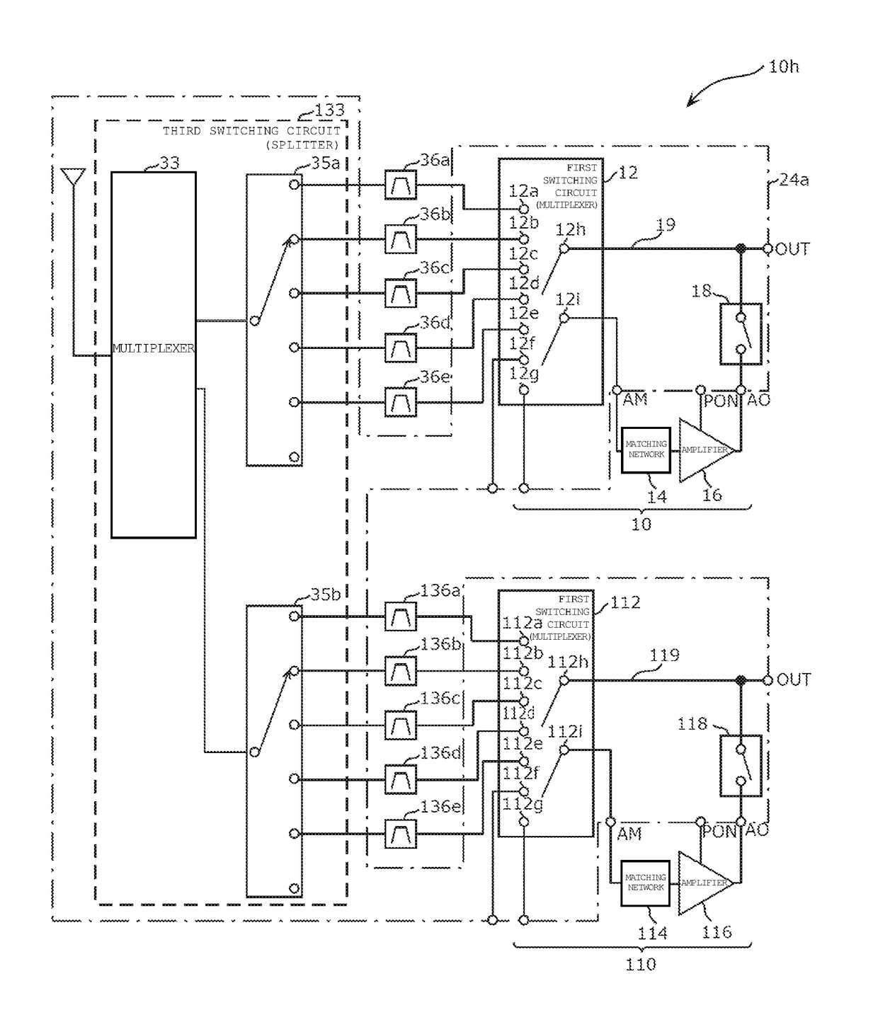
[0094]FIG. 1 is a circuit diagram of an amplification circuit of preferred embodiment 1 of the present invention. The amplification circuit 10 preferably is a bypass-path-equipped amplification circuit and includes a first switching circuit 12, a matching network 14, an amplifier 16, a second switching circuit 18 and a bypass path 19.

[0095]The first switching circuit 12 is a circuit that includes one or more input terminals (here, input terminals 12a to 12g that correspond to signals a to g of a plurality of frequency bands), and a first output terminal 12i and a second output terminal 12h and that puts the second output terminal 12h into an open state of being open with respect to the input terminals 12a to 12g while selectively connecting the first output terminal 12i to any one of the input terminals 12a to 12g or selectively connects the second output terminal 12h to any one of the input terminals 12a to 12g while putting the first output terminal 12i into ...

embodiment 2

Preferred Embodiment 2

[0122]Next an amplification circuit of preferred embodiment 2 of the present invention will be described.

[0123]FIG. 7 is a circuit diagram of an amplification circuit of preferred embodiment 2 of the present invention. The amplification circuit 30 is a high-frequency module that selects and amplifies one signal from among signals of a plurality of frequency bands received by an antenna and includes a third switching circuit 32, a control circuit 34 and filters 36a to 36e in addition to the constituent components of the amplification circuit 10 of preferred embodiment 1.

[0124]The third switching circuit 32 is a circuit that includes an input terminal 32a and a plurality of output terminals 32b to 32h and that selectively connects the input terminal 32a to any of the plurality of output terminals 32b to 32h in accordance with a control signal input from the control circuit 34, and is, for example, a splitter includes a single pole n throw (SPnT; n being the numbe...

embodiment 3

Preferred Embodiment 3

[0145]Next an amplification circuit of preferred embodiment 3 of the present invention will be described.

[0146]FIG. 10 is a circuit diagram of an amplification circuit 10b of preferred embodiment 3 of the present invention. The amplification circuit 10b is a high-frequency module that selects and amplifies one signal from among signals of a plurality of frequency bands received by an antenna. The amplification circuit 10b includes a configuration in which, in the amplification circuit 10 of preferred embodiment 1, the amplifier 16 is replaced with an amplifier 16a which is a variable-gain amplifier. Elements which are the same as those in preferred embodiment 1 are denoted by the same reference symbols, and primarily different points will be described.

[0147]The amplifier 16a is connected to the output side of the matching network 14 and is preferably, for example, a low-noise amplifier of variable gain manufactured using an Si—Ge process. The gain of the amplif...


PUM


Abstract

An amplification circuit includes a first switching circuit that includes input terminals and first and second output terminals and that puts the second output terminal into an open state with respect to the input terminals while selectively putting the first output terminal into a state of being connected to any of the input terminals or selectively puts the second output terminal into a state of being connected to any of input terminals while putting the first output terminal into a state of being open with respect to the input terminals; a matching network that is connected to the first output terminal; an amplifier that is connected to an output side of the matching network; a second switching circuit that is connected to an output side of the amplifier; and a bypass path that electrically connects the second output terminal and an output terminal of the second switching circuit. The amplifier is a variable-gain amplifier.

Description

CROSS REFERENCE TO RELATED APPLICATIONS[0001]This application claims the benefit of priority to Japanese Patent Application 2016-079139 filed Apr. 11, 2016 and Japanese Patent Application 2015-133914 filed Jul. 2, 2015. The entire contents of each application are hereby incorporated by reference.BACKGROUND OF THE INVENTION1. Field of the Invention[0002]The present invention relates to an amplification circuit and in particular relates to an amplification circuit that selectively inputs an input signal to an amplifier and selectively bypasses an amplifier.2. Description of the Related Art[0003]There are amplification circuits, which are for an input signal received from an antenna or the like, in which processing is performed to cause an input signal to be input to and amplified by a low-noise amplifier in the case in which the input signal is a low-power signal and to cause the input signal to bypass the low-noise amplifier in the case in which the input signal is a high-power signa...

Claims


Application Information

Patent Timeline
Patent Type & Authority Applications(United States)
IPC IPC(8): H03F3/217H03F3/00H03F1/56H03F3/04H03F1/30
CPCH03F3/2178H03F3/005H03F1/56H03F1/303H03F3/04H03F3/195H03F3/72H03F2200/111H03F2200/222H03F2200/294H03F2203/7209H03F2203/7233H03F2203/7236H03F2203/7239H03F1/565H03F3/191H03F1/0288H03F3/211H03F1/0277
Inventor OSHITA, TERUAKI
Owner MURATA MFG CO LTD
Why Eureka
Try Eureka