Semiconductor light emitting devices

a technology of light-emitting devices and semiconductors, which is applied in the direction of semiconductor devices, basic electric elements, electrical appliances, etc., can solve the problems of color variation and decrease in the final optical efficiency of products, and achieve the effect of improving optical efficiency and reducing and/or minimizing optical loss

Active Publication Date: 2017-10-26
SAMSUNG ELECTRONICS CO LTD
View PDF6 Cites 19 Cited by
  • Summary
  • Abstract
  • Description
  • Claims
  • Application Information

AI Technical Summary

Benefits of technology

[0005]Some aspects of the present inventive concepts may provide a semiconductor light e...

Problems solved by technology

In an SP packaging process of such LEDs, optical loss or total reflection due to other components may cau...

Method used


Image

  • Semiconductor light emitting devices
  • Semiconductor light emitting devices
  • Semiconductor light emitting devices

Examples


Embodiment Construction

[0031]Hereinafter, example embodiments of the present inventive concepts will be described in detail with reference to the attached drawings.

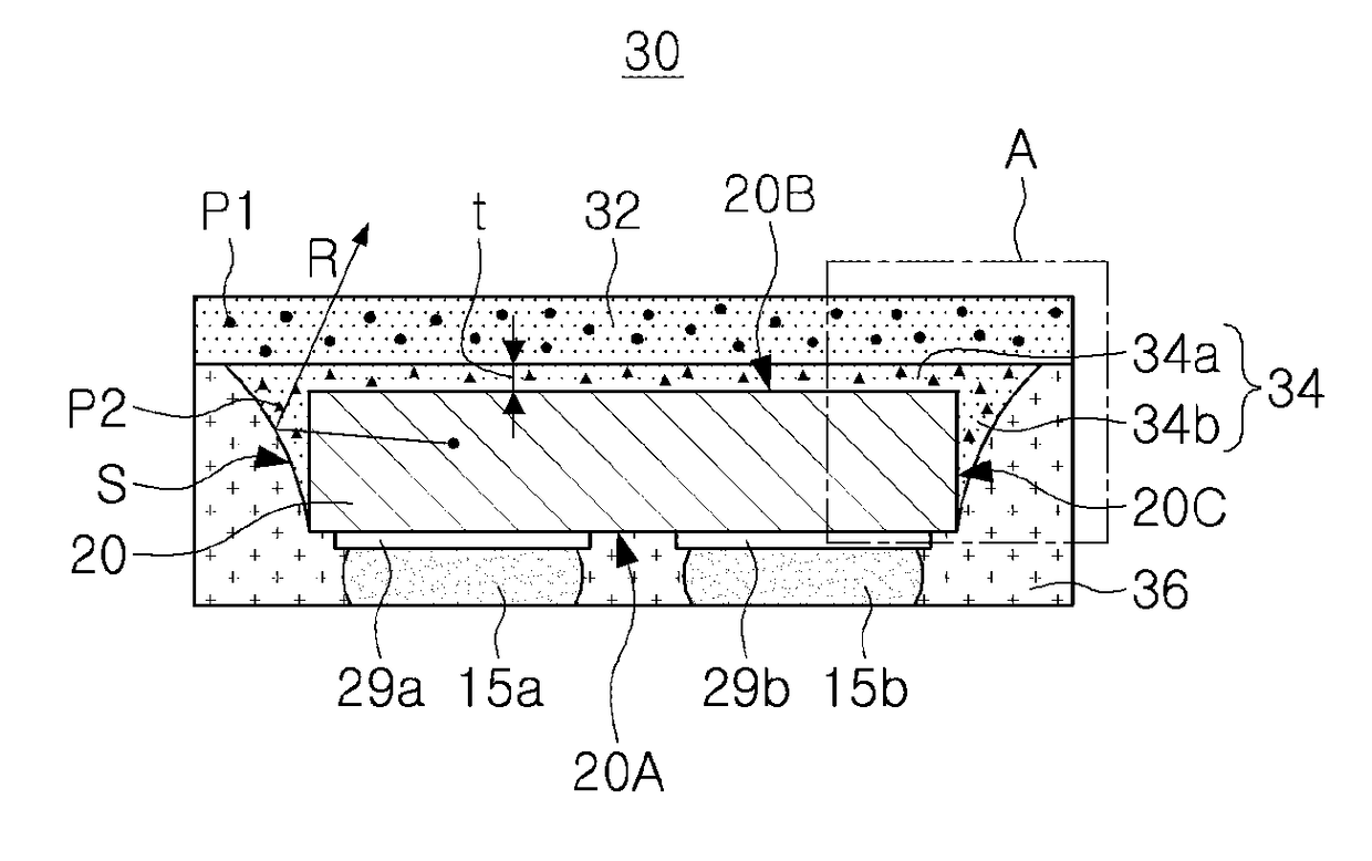
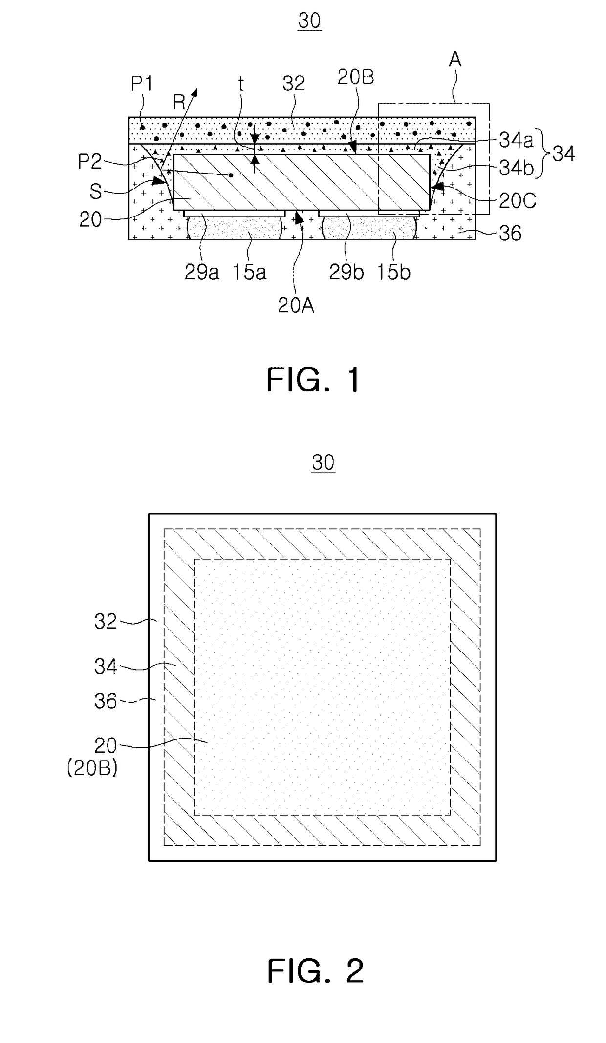
[0032]FIG. 1 is a cross-sectional view of a semiconductor light emitting device according to some example embodiments of the present inventive concepts. FIG. 2 is a plan view of the semiconductor light emitting device illustrated in FIG. 1.

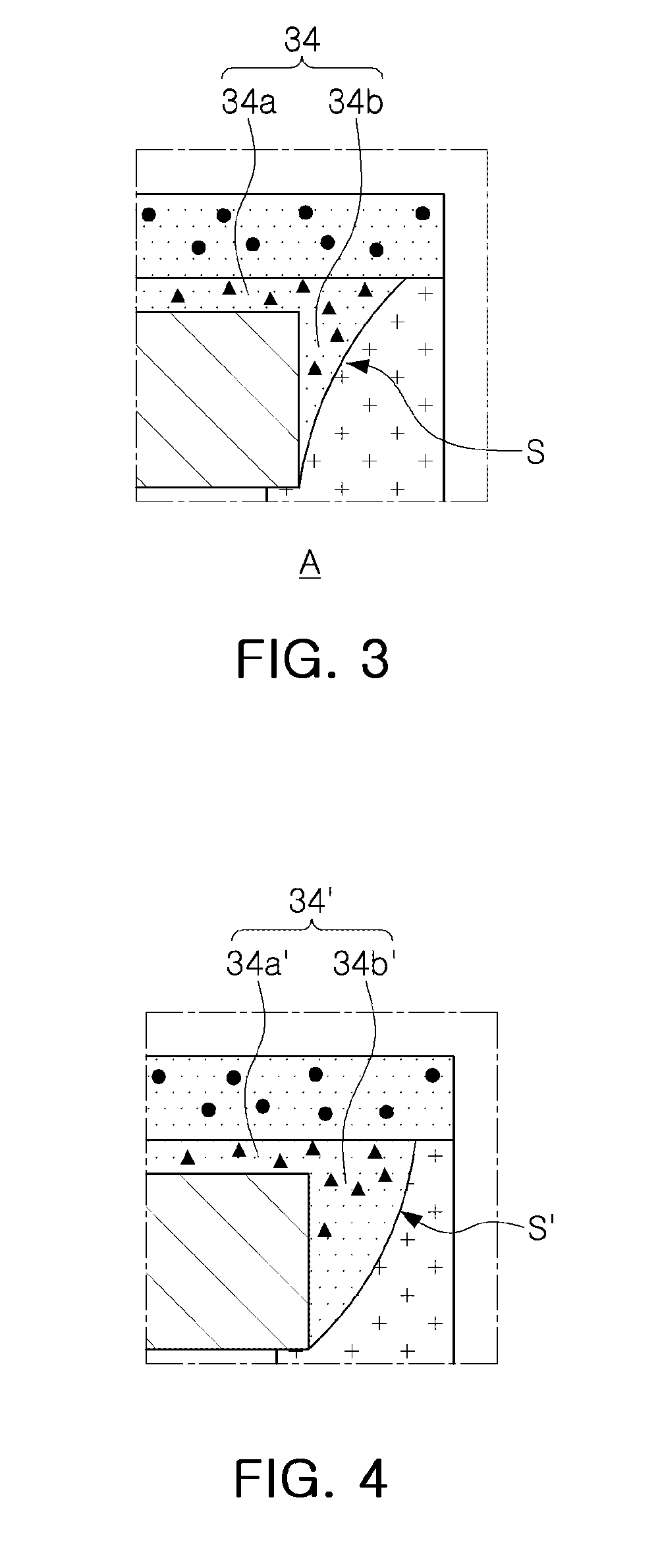
[0033]Referring to FIG. 1, a semiconductor light emitting device 30 according to some example embodiments may include a semiconductor light emitting diode (LED) chip 20, a light-transmitting film 32 disposed on a surface of the semiconductor LED chip 20, and a light-transmitting bonding layer 34 bonding the semiconductor LED chip 20 to the light-transmitting film 32.

[0034]The semiconductor LED chip 20 may have a first surface 20A, a second surface 20B opposing the first surface 20A, and at least one lateral surface 20C disposed in a space between the first surface 20A and the second surface 20B. The first sur...


PUM


Abstract

A semiconductor light emitting device may include a semiconductor light emitting diode (LED) chip, a light-transmitting film on the LED chip, and a light-transmitting bonding layer between the light-transmitting film and the semiconductor LED chip. At least one of the light-transmitting film and the light-transmitting bonding layer may include a wavelength conversion material configured to convert light emitted by the semiconductor LED chip into light having a wavelength different from a wavelength of the emitted light. The light-transmitting bonding layer may have a lateral inclined region extending to the lateral surface to form an inclined surface. The semiconductor light emitting device may further include a reflective packaging portion surrounding the light-transmitting bonding layer, covering the first surface such that an electrode of the LED chip is at least partially exposed. The reflective packaging portion may include a reflective material.

Description

CROSS-REFERENCE TO RELATED APPLICATIONS[0001]This application claims benefit of priority to Korean Patent Application No. 10-2016-0050215, filed on Apr. 25, 2016 in the Korean Intellectual Property Office, the disclosure of which is incorporated herein by reference in its entirety.BACKGROUND1. Field[0002]The present inventive concepts relate to semiconductor light emitting devices.2. Description of Related Art[0003]Semiconductor light emitting diodes (LEDs) may include materials included therein that are configured to emit light using electric energy. Semiconductor LEDs may convert energy, generated by a recombination of electrons and holes of bonded semiconductors, into light, and emit the light. Such LEDs are widely used as light sources of lighting devices and backlight devices for large liquid crystal displays, and development of the LEDs is being gradually accelerated.[0004]In some cases, LEDs may be provided as light emitting devices packaged in various forms so as to be easil...

Claims


Application Information

Patent Timeline
IPC IPC(8): H01L33/50H01L33/38H01L33/46H01L33/62
CPCH01L33/504H01L33/46H01L33/38H01L33/62H01L33/22H01L33/58H01L33/60H01L2933/0058H01L2933/0041H01L33/508H01L33/56H01L33/50H01L33/505H01L33/005H01L33/52H01L2924/12041H01L2933/005H01L33/502
Inventor SEO, JONG WANKIM, JIN HAWOO, KWANG BOKLEE, DONG HOONLEE, WON JOONHWANG, SUN HWAN
Owner SAMSUNG ELECTRONICS CO LTD
Why Eureka
Try Eureka