
Source/drain performance through conformal solid state doping

a technology of solid state doping and source/drain, applied in the direction of semiconductor devices, electrical equipment, transistors, etc., can solve the problems of challenging the ion implantation process of finfet and nanowire devices

Active Publication Date: 2017-11-02
ASM IP HLDG BV
View PDF0 Cites 297 Cited by
  • Summary
  • Abstract
  • Description
  • Claims
  • Application Information

AI Technical Summary

Benefits of technology

The invention provides a method for making a semiconductor device for source / drain applications. The method involves cleaning the substrate, depositing a dopant layer, and depositing a capping layer. This process forms a channel material for NMOS and CMOS devices. The technical effects of this method include improved dopant diffusion and reduced oxidation during the process. The method is efficient and effective for producing high-quality semiconductor devices.

Problems solved by technology

However, the ion implantation process can be challenging for FinFET and nanowire devices.

Method used


Image

  • Source/drain performance through conformal solid state doping
  • Source/drain performance through conformal solid state doping
  • Source/drain performance through conformal solid state doping

Examples


Embodiment Construction

[0015]Although certain embodiments and examples are disclosed below, it will be understood by those in the art that the invention extends beyond the specifically disclosed embodiments and / or uses of the invention and obvious modifications and equivalents thereof. Thus, it is intended that the scope of the invention disclosed should not be limited by the particular disclosed embodiments described below.

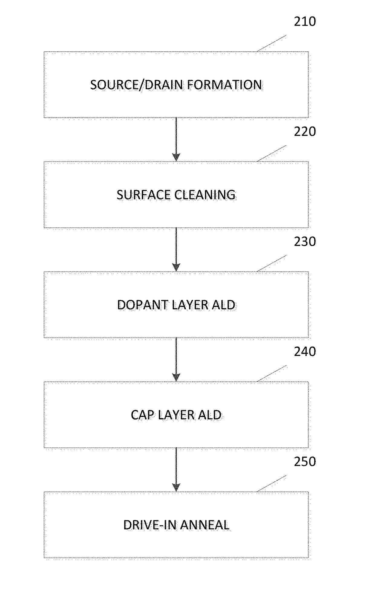
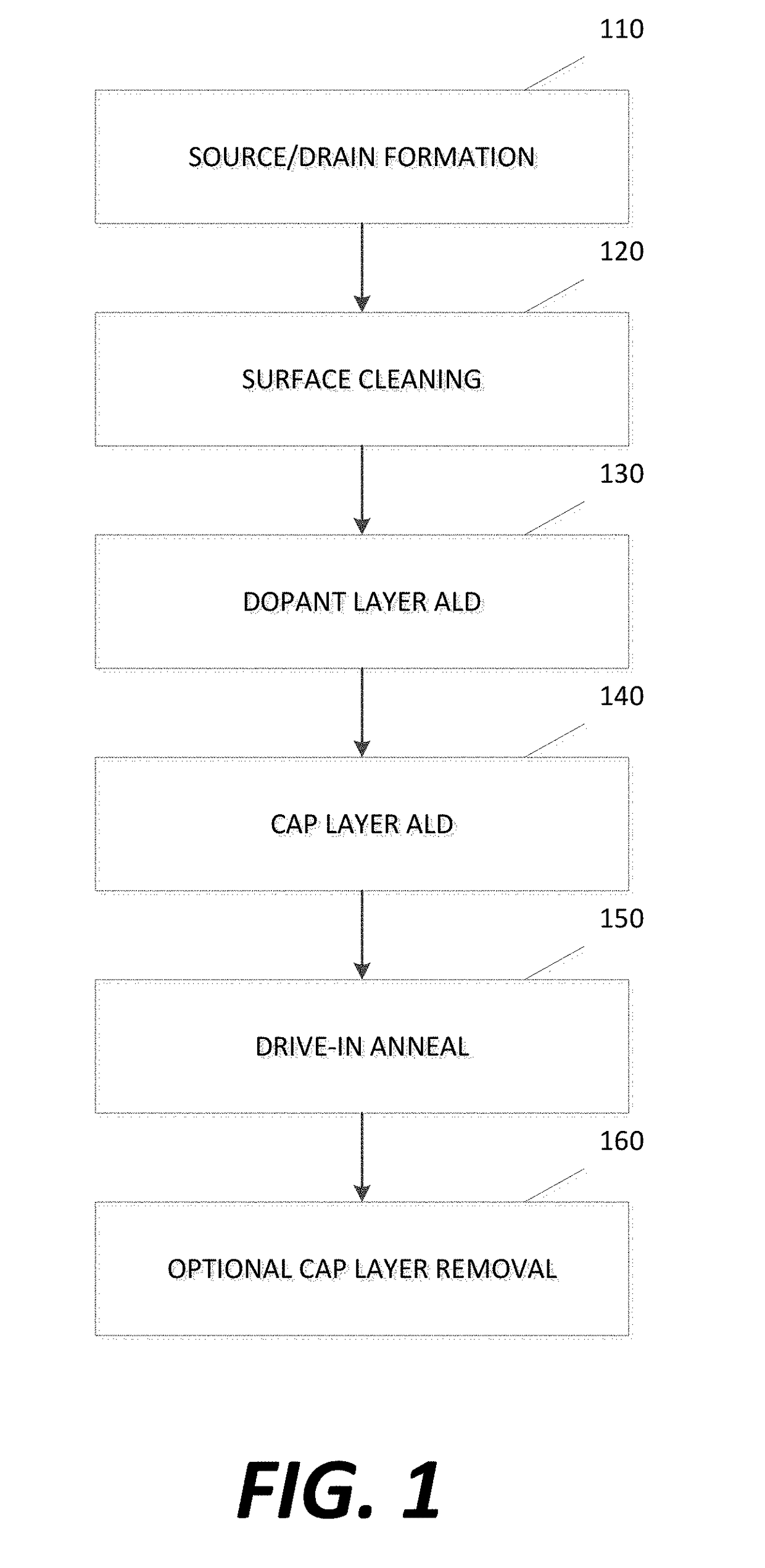
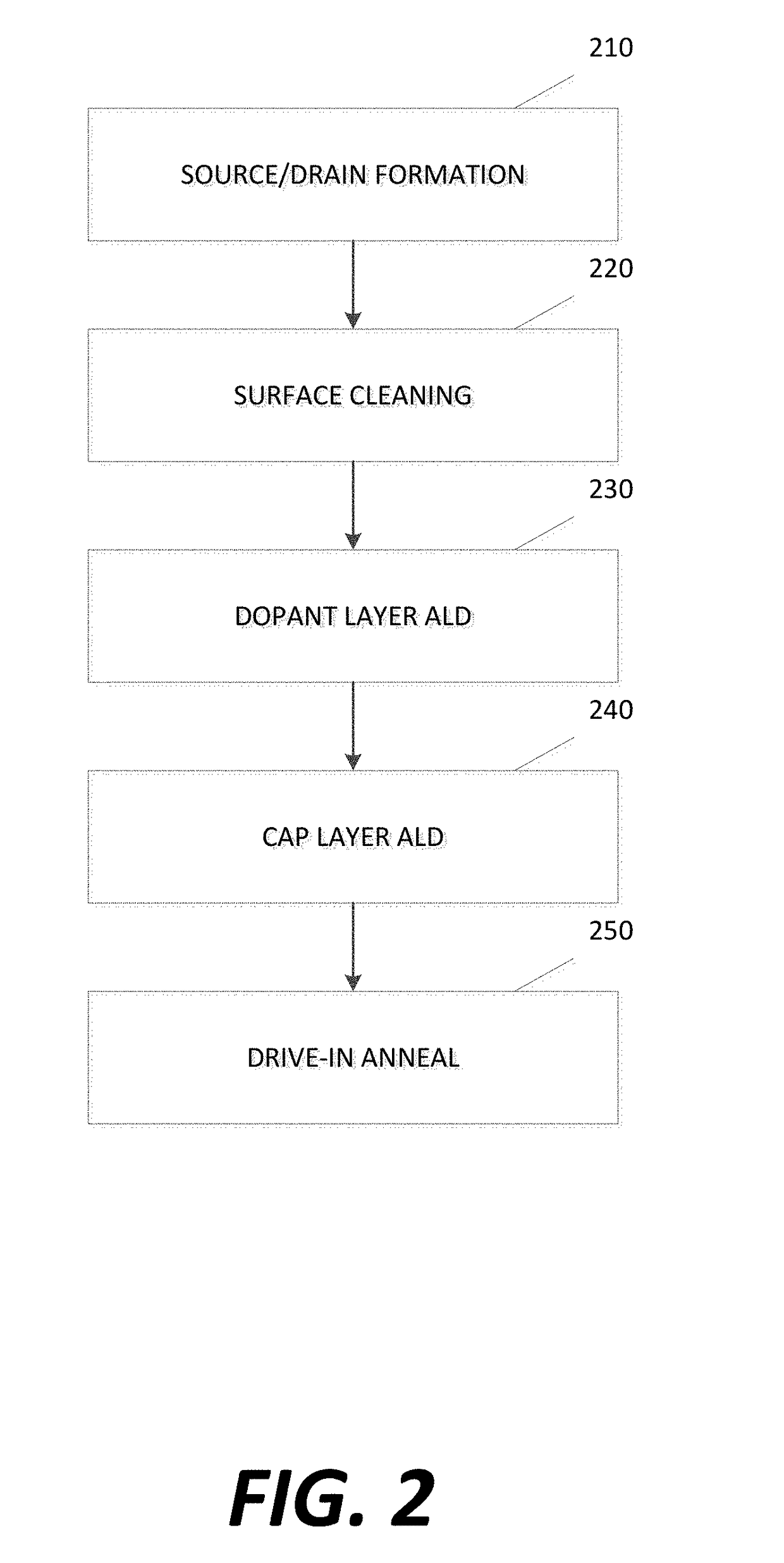
[0016]Atomic layer deposition (ALD) solid state doping (SSD) may be one way to form NMOS and CMOS devices. One reason for this may be the ability of ALD SSD to form films with excellent conformality and defect free features. Alternate doping methods, such as ion implantation, may introduce defects that ALD SSD can avoid during conformal doping of 3-D structures. ALD SSD also may provide the capability to deposit thin films with precise sub-nanometer thickness control, which thus determines the dose or number of atoms available at the surface to incorporate into the semiconductor as act...


PUM


Abstract

A method for improving source / drain performance through conformal solid state doping and its resulting device are disclosed. Specifically, the doping takes place through an atomic layer deposition of a dopant layer. Embodiments of the invention may allow for an increased doping layer, improved conformality, and reduced defect formation, in comparison to alternate doping methods, such as ion implantation or epitaxial doping.

Description

CROSS-REFERENCE TO RELATED APPLICATION[0001]This application is related to U.S. Non-provisional patent application Ser. No. 13 / 504,079, filed on Sep. 17, 2012, entitled “Synthesis and Use of Precursors for ALD of Group VA Element Containing Thin Films,” and issued as U.S. Pat. No. 9,315,896, the disclosure of which is hereby incorporated by reference in its entirety.FIELD OF INVENTION[0002]The present disclosure generally relates to processes for manufacturing electronic devices. More particularly, the disclosure relates to forming source / drain devices for NMOS and CMOS applications. Specifically, the disclosure discloses methods to improve a source / drain doping level with a conformal solid state doping technique.BACKGROUND OF THE DISCLOSURE[0003]Germanium has been considered as an appropriate material for use in CMOS and NMOS devices. With the trend towards smaller devices, contact area on the devices has become smaller, with a substantial increase in contact resistance. The increa...

Claims


Application Information

Patent Timeline
IPC IPC(8): H01L21/02H01L29/36H01L21/265H01L29/417
CPCH01L21/0262H01L21/02694H01L29/41725H01L29/36H01L21/26506H01L21/02532H01L21/02658H01L21/2254H01L29/0847H01L21/0228H01L21/324H01L29/6659H01L21/02205
Inventor XIE, QIDE ROEST, DAVIDWOODRUFF, JACOBGIVENS, MICHAEL EUGENEMAES, JAN WILLEMBLANQUART, TIMOTHEE
Owner ASM IP HLDG BV
Learn More