Semiconductor Device and Method for Producing a Plurality of Semiconductor Devices

Active Publication Date: 2017-11-23
OSRAM OLED
View PDF2 Cites 1 Cited by
  • Summary
  • Abstract
  • Description
  • Claims
  • Application Information

AI Technical Summary

Benefits of technology

[0042]Furthermore, the semiconductor chips on the rear side are free of material of the molding and thus freely accessible, for example, for electrical and/or thermal contacting, for example, by a contact t

Problems solved by technology

These requirements cannot be achiev

Method used


Image

  • Semiconductor Device and Method for Producing a Plurality of Semiconductor Devices
  • Semiconductor Device and Method for Producing a Plurality of Semiconductor Devices
  • Semiconductor Device and Method for Producing a Plurality of Semiconductor Devices

Examples


Embodiment Construction

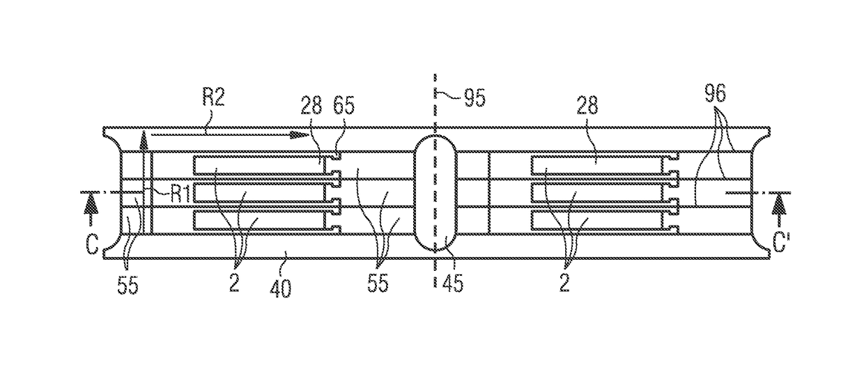
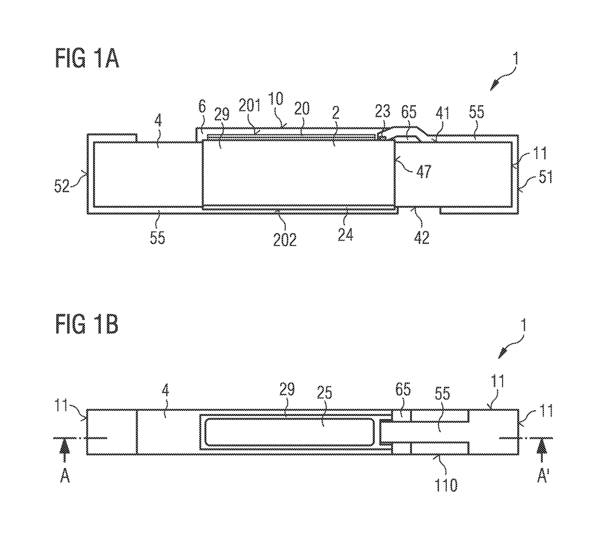
[0056]A first exemplary embodiment of a semiconductor device 1 is shown schematically in FIGS. 1A and 1B.

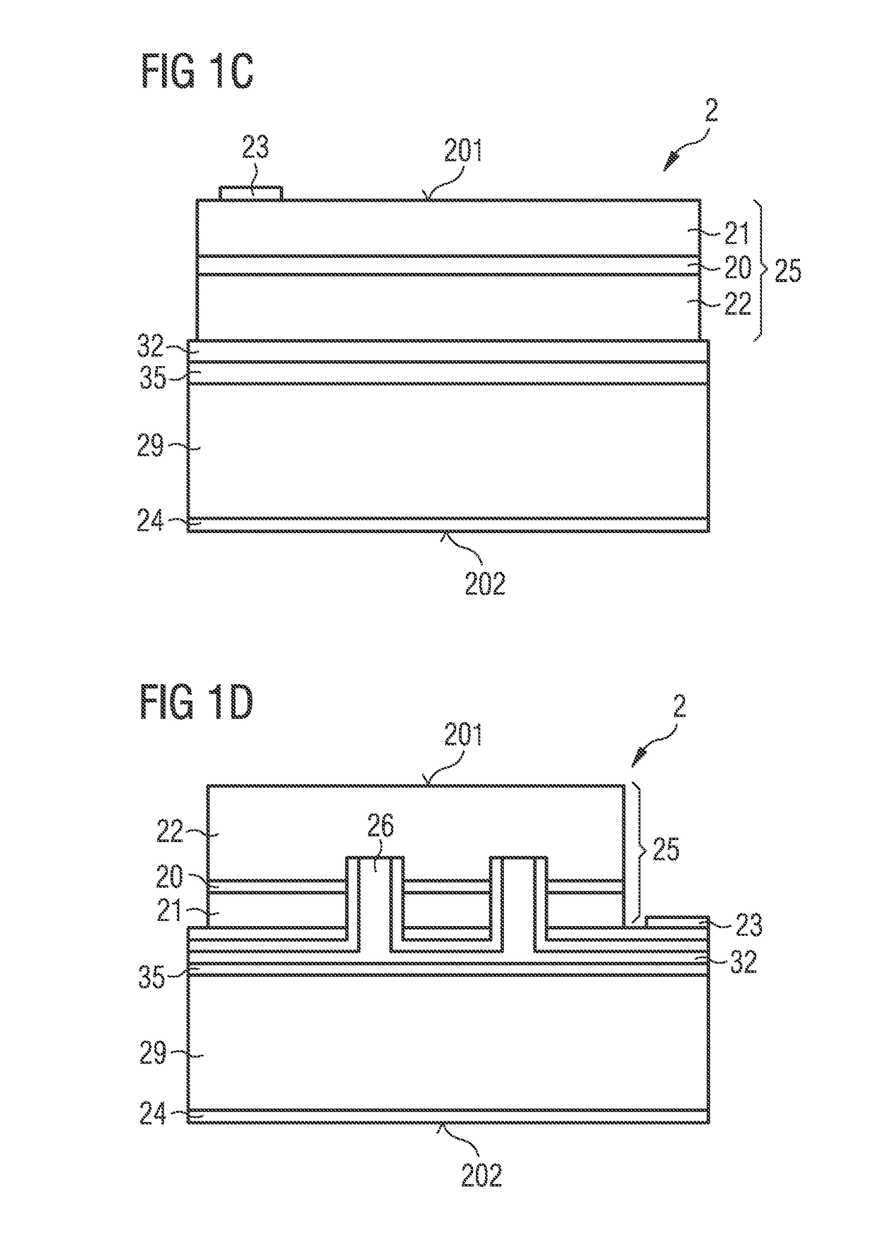
[0057]The semiconductor device 1 has a semiconductor chip 2 provided for generating radiation with a semiconductor layer sequence 25. The semiconductor layer sequence has an active region 20 provided for generating radiation. A radiation exit surface 10 of the semiconductor device runs parallel to the main extension plane of the active region. Details of the semiconductor chip 2 are explained in greater detail with reference to two exemplary embodiments in connection with FIGS. 1C and 1D.

[0058]Molded onto the semiconductor chip 2 is a molding 4. The molding 4 is used for the mechanical stabilization of the semiconductor chip and forms a housing for the semiconductor chip. The molding extends perpendicular to the radiation exit surface 10 between a rear side 42 of the molding lying opposite the radiation exit surface and a front side 41 of the molding. At the places at which the m...


PUM


Abstract

A semiconductor device and a method for producing a plurality of semiconductor devices are disclosed. In an embodiment an optoelectronic semiconductor device includes a semiconductor chip having a semiconductor layer sequence with an active region, a radiation exit surface arranged parallel to the active region and a plurality of side faces arranged obliquely or perpendicular to the radiation exit surface. The device further includes a contact track electrically connecting the semiconductor chip to a contact surface configured to externally contact the semiconductor device, a molding and a rear side of the semiconductor chip remote from the radiation exit surface, the rear side being free of a material of the molding, wherein one of the side faces is configured as a mounting side face for fastening of the semiconductor device, and wherein the contact track runs on one of the side faces in places.

Description

[0001]This patent application is a national phase filing under section 371 of PCT / EP2015 / 078708, filed Dec. 4, 2015, which claims the priority of German patent application 10 2014 118 349.5, filed Dec. 10, 2014, each of which is incorporated herein by reference in its entirety.TECHNICAL FIELD[0002]The present application relates to an optoelectronic semiconductor device and a method for producing a plurality of optoelectronic semiconductor devices.BACKGROUND[0003]In handheld electronic devices, such as mobile telephones, for example, liquid crystal displays are often used, which are backlit by light-emitting diodes (LEDs) radiating laterally into light guides. In a reduction in the weight and depth of such devices, the light guides and LEDs must also be miniaturized further. In addition, it must be possible to produce the LEDs inexpensively. These requirements cannot be achieved easily with conventional designs.SUMMARY OF THE INVENTION[0004]One object is to specify an optoelectronic...

Claims


Application Information

Patent Timeline
IPC IPC(8): H01L33/48H01L23/00H01L33/54H01L33/60H01L33/62H01L33/00
CPCH01L33/486H01L33/60H01L33/54H01L33/62H01L2933/005H01L24/95H01L2224/01H01L2924/181H01L2933/0033H01L33/0079H01L2924/0002H01L21/568H01L2224/24H01L2224/82H01L2224/06181H01L33/0093H01L2224/96
Inventor SCHWARZ, THOMASSINGER, FRANK
Owner OSRAM OLED
Why Eureka
Try Eureka