Unlock instant, AI-driven research and patent intelligence for your innovation.

amplifier

Active Publication Date: 2017-11-23
SONY CORP
View PDF1 Cites 0 Cited by
  • Summary
  • Abstract
  • Description
  • Claims
  • Application Information

AI Technical Summary

Benefits of technology

The technology described in the patent text can reduce noise in an output signal without affecting the signal-to-noise ratio. This means that the technology can improve the quality of the output signal.

Problems solved by technology

However, the signal amplifier circuit is a noise source, and therefore, the noise generated from the signal amplifier when a received signal is amplified is superimposed on the signal.

Method used


Image

  • amplifier
  • amplifier
  • amplifier

Examples


second embodiment

(B) Second Embodiment

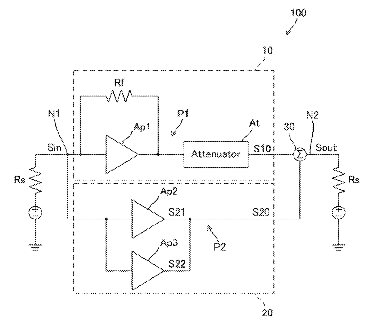
[0032]FIG. 2 is a diagram for explaining the configuration of an amplifier 200 according to this embodiment. The amplifier 200 shown in the drawing includes a first amplifier 210, an attenuator 220, a second amplifier 230, a third amplifier 240, and an adder 250.

[0033]The first amplifier 210 has the configuration of a CMOS inverter that serves as a first transistor unit in which a power supply terminal of a voltage Vdd and a power supply terminal of a ground Gnd are connected by a p-channel MOS transistor (hereinafter referred to as pMOS) M1 and an n-channel MOS transistor (hereinafter referred to as nMOS) M2. The first amplifier 210 outputs a signal S11 generated by inverting and amplifying an input signal Sin of an input node N1. That is, the gate of the pMOS M1 forming the first amplifier 210 is connected to the input node N1, the drain of the pMOS M1 is connected to the power supply terminal of the voltage Vdd, and the source of the pMOS M1 is connected, via...

third embodiment

(C) Third Embodiment

[0048]Next, an amplifier 300 with a wider bandwidth and a lower voltage than those of the above described amplifier 200 according to the second embodiment is described. FIG. 4 is a diagram for explaining the configuration of the amplifier 300 according to this embodiment. It should be noted that, in this embodiment, the same components as those of the above described amplifier 200 according to the second embodiment are denoted by the same reference numerals as those used in the second embodiment, and detailed explanation of them will not be made below.

[0049]The amplifier300 differs from the above described circuit configuration according to the second embodiment in that the MOS transistors forming the first amplifier 210 and the second amplifier 230 are cascoded. It should be noted that this embodiment will be described below through an example case where the pMOSs with the larger size between the nMOSs and the pMOSs of the respective CMOSs forming the first ampl...


PUM


Abstract

An output signal can be free of any noise component generated from an amplifier disposed in a path, without degradation of the S / N ratio of the output signal. An amplifier includes: a first amplifier that is connected to an input node and generates a first intermediate signal; a feedback resistor that enables feedback of the first intermediate signal to the input node; an attenuator that receives the first intermediate signal and generates a second intermediate signal; a second amplifier that is connected to the input node and generates a third intermediate signal; a third amplifier that is connected to the input node and generates a fourth intermediate signal; and an adder that generates an output signal, using the second intermediate signal, the third intermediate signal, and the fourth intermediate signal.

Description

TECHNICAL FIELD[0001]The present technology relates to amplifiers.BACKGROUND ART[0002]A communication device such as an RF receiver includes a signal amplifier circuit for amplifying received signals. In such a communication device, it is critical to increase the S / N ratio by reducing noise. However, the signal amplifier circuit is a noise source, and therefore, the noise generated from the signal amplifier when a received signal is amplified is superimposed on the signal. Patent Document 1 discloses a technology for reducing noise generated from the signal amplifier in such a communication device.[0003]FIG. 6 is a diagram for explaining a conventional noise reduction technology according to Patent Document 1.[0004]The circuit shown in the drawing includes: a first amplifier Ap1 that is connected to an input node and generates a first intermediate signal; a feedback resistor Rf that enables feedback of the first intermediate signal to the input node; a first attenuator At1 that rece...

Claims


Application Information

Patent Timeline
Patent Type & Authority Applications(United States)
IPC IPC(8): H03F1/26H03F3/193H03F1/22H03F3/68H03G1/00
CPCH03F1/26H03F3/193H03G2201/106H03G1/0094H03F3/68H03F1/223H03F3/211H03F3/3022H03F2200/294H03F2200/372H03F2200/451H03G1/0088
Inventor TAKAHASHI, KATSUAKITAKANO, HIDEYUKIYOSHIKAWA, NAOTO
Owner SONY CORP