Element chip manufacturing method

Active Publication Date: 2017-11-30
PANASONIC INTELLECTUAL PROPERTY MANAGEMENT CO LTD
View PDF3 Cites 4 Cited by
  • Summary
  • Abstract
  • Description
  • Claims
  • Application Information

AI Technical Summary

Benefits of technology

The present invention provides a method to prevent degradation or damage to bumps on a substrate during plasma dicing without reducing productivity. This is achieved by forming a resist mask covering the bumps and including an opening in the dividing region. The resist mask needs to be thick enough to not expose the bumps during plasma dicing. This method significantly increases the use amount of resist solution, the time required for resist mask formation and production cost. Additionally, a method of suppressing bump degradation or damage by plasma during substrate singulation is also provided.

Problems solved by technology

When the scattered metal is deposited to the inside of the plasma processing apparatus, generation of plasma may become unstable or the substrate which is a plasma dicing target may be contaminated with metal.
The scattered metal is deposited to the substrate again or a portion of the bump is etched such that reduction in electrical device characteristics and reliability of an element chip to be obtained may be caused.
Accordingly, a use amount of the resist solution is significantly increased, the time required for formation of the resist mask is increased, and production cost is increased.
When the resist mask is thick, the time required for plasma ashing becomes longer and thus, productivity is reduced.
The head top part of the bump is exposed to plasma for a long time during plasma ashing and thus, the surface of the bump is easily oxidized.
Accordingly, deterioration of device characteristics, for example, increase in contact resistance of the substrate is easily generated.
As such, in a case where the bump is covered with the resist mask in order to suppress the bump from being irradiated with plasma, there is a problem from productivity and device characteristics point of view.

Method used


Image

  • Element chip manufacturing method
  • Element chip manufacturing method
  • Element chip manufacturing method

Examples


first exemplary embodiment

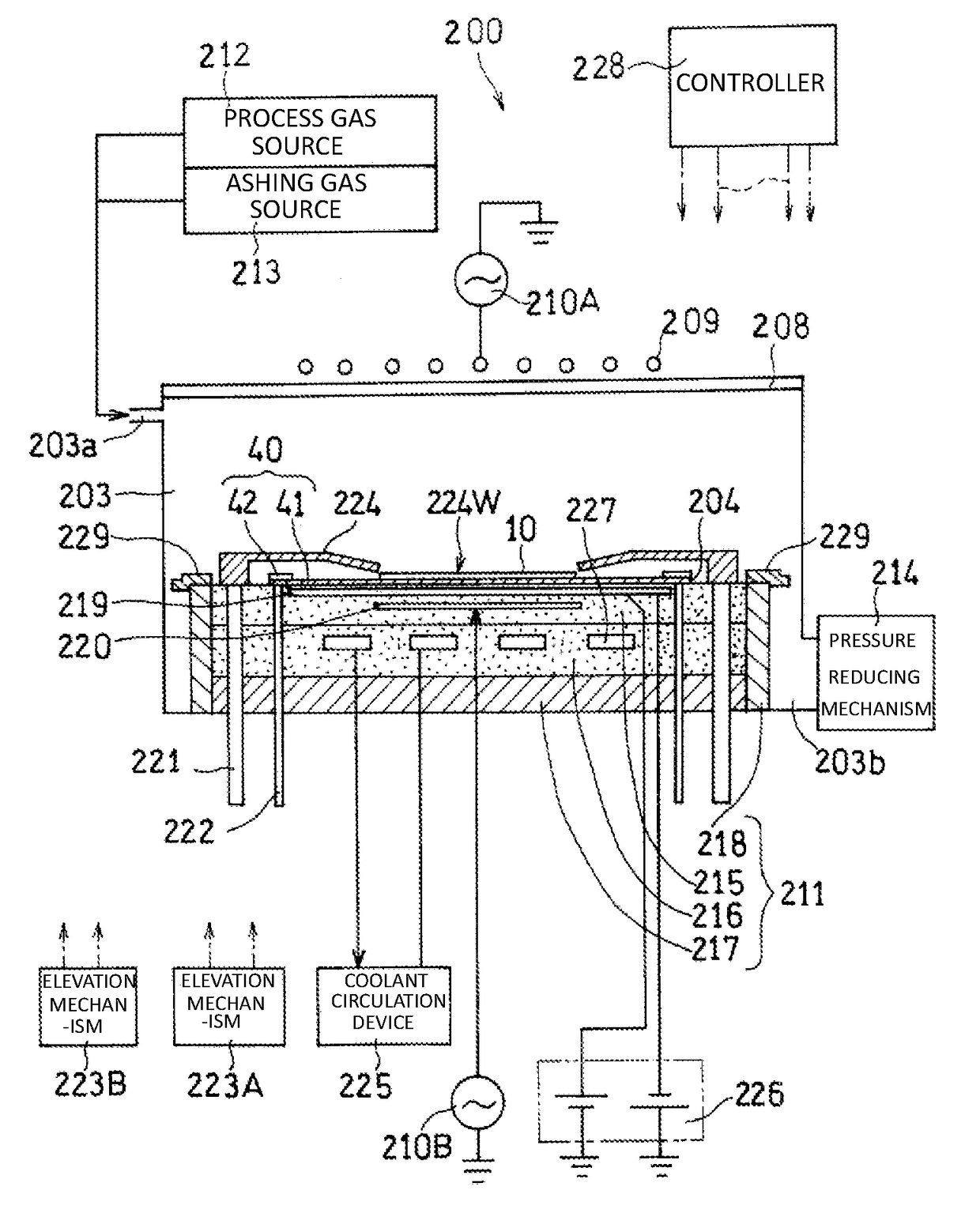
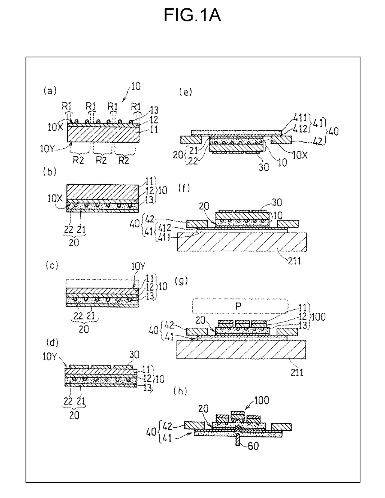
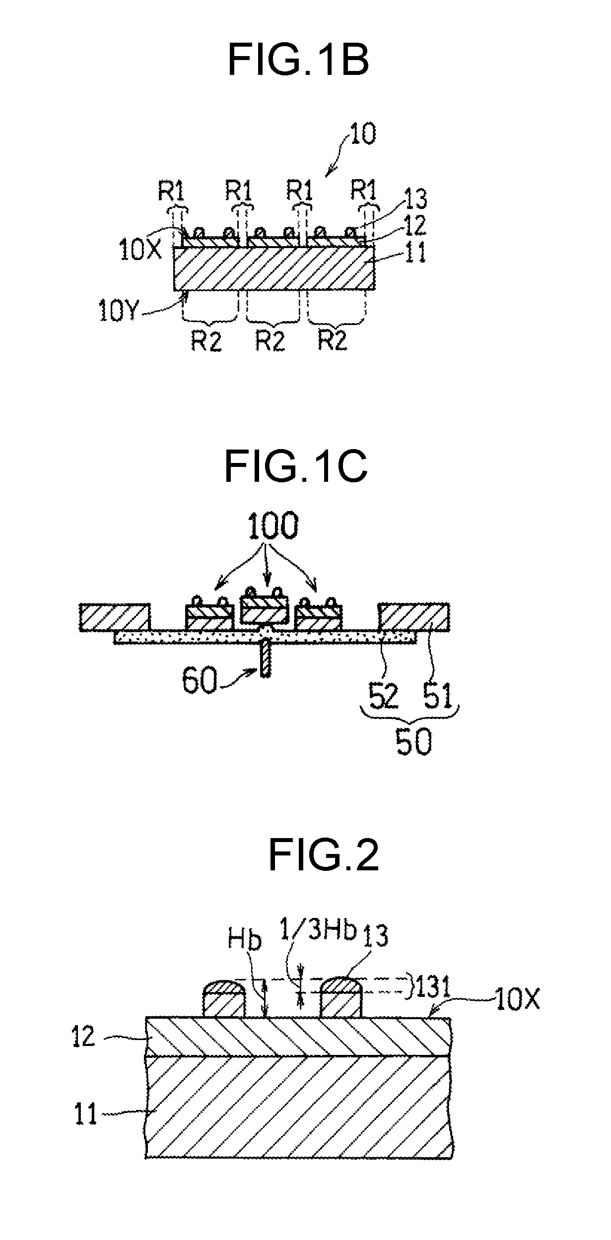
[0032]In the present exemplary embodiment, a bump embedding process is performed by adhering a protection tape having an adhesive layer to a first surface. A manufacturing method according to the present exemplary embodiment will be described with reference to FIG. 1A to FIG. 5. (a) to (h) of FIG. 1A are conceptual diagrams illustrating a manufacturing method according to the present exemplary embodiment using a cross section of a substrate. FIG. 1B is a cross-sectional view illustrating another example of the substrate used in the present exemplary embodiment. FIG. 1C is a conceptual diagram illustrating another example of a bump exposing process conducted in the present exemplary embodiment using a cross section of the substrate. FIG. 2 is a cross-sectional view schematically illustrating a configuration of the substrate (before thinning process) according to the present exemplary embodiment. FIG. 3A is a cross-sectional view schematically illustrating a laminated structure formed...

second exemplary embodiment

[0090]The present exemplary embodiment is similar to the first exemplary embodiment except that except that after the mask forming process, protection tape 20 is peeled off from first surface 10X and holding tape 41 is adhered to first surface 10X so as to embed bump 13 into second adhesive layer 412 of holding tape 41. In FIG. 6, a manufacturing method of an element chip of the present exemplary embodiment is illustrated ((a) to (h)). (a) to (d) and (h) of FIG. 6 respectively correspond to (a) to (d) of FIG. 1A and FIG. 1C.

[0091]In the present exemplary embodiment, after the mask forming process ((d) of FIG. 6), protection tape 20 is peeled off from first surface 10X and holding tape 41 supported on frame 42 is adhered to first surface 10X so as to embed at least head top part 131 of bump 13 into second adhesive layer 412 of holding tape 41 ((e) of FIG. 6). That is, the bump embedding process and the holding process are conducted at the same time. With this, the processes are simpl...


PUM


Abstract

An element chip manufacturing method includes a preparation process of preparing a substrate which includes a first surface having an exposed bump and a second surface opposite to the first surface and includes a plurality of element regions defined by dividing regions, a bump embedding process of embedding at least a head top part of the bump into the adhesive layer, a mask forming process of forming a mask in the second surface. The method for manufacturing the element chip includes a holding process of arranging the first surface to oppose a holding tape supported on a frame and holding the substrate on the holding tape, a placement process of placing the substrate on a stage provided inside of a plasma processing apparatus through the holding tape, after the mask forming process and the holding process.

Description

BACKGROUND OF THE INVENTION1. Field of the Invention[0001]The present disclosure is related to a method for manufacturing an element chip by singulating a substrate which includes a bump.2. Description of the Related Art[0002]As a method for singulating a substrate including a plurality of element regions defined by dividing regions, a method (plasma dicing) for plasma etching the dividing regions to a depth which extends from one surface of the substrate to the other surface is known. The substrate, in general, includes a semiconductor layer, a circuit layer laminated on the semiconductor layer, and a projection (bump) disposed on the circuit layer and containing a metallic element such as an electrode pad (bonding pad) and a solder ball. An element chip including the circuit layer and the bump is formed by plasma etching the dividing regions of the substrate.[0003]The plasma dicing is performed by placing the substrate on a stage installed in a plasma processing apparatus. General...

Claims


Application Information

Patent Timeline
IPC IPC(8): H01L23/00H01L23/498H01L21/687H01L21/67H01L21/48H05K13/04B44C1/22
CPCH01L24/11H01L24/13H01L21/4853H01L21/68742H05K13/0465B44C1/227H01L21/67069H01L23/49811H01L21/02H01L21/02002H01L2224/11H01L2221/68327H01L2224/13101H01L21/6835H01L21/78H01L2224/13013H01L2224/13014H01L2224/13111H01L2224/13124H01L2224/13139H01L2224/13147H01L21/30655H01L21/31138H01L21/32136H01L2924/014
Inventor HARIKAI, ATSUSHIOKITA, SHOGOITOU, AKIHIROTAKANO, KATSUMIHIROSHIMA, MITSURU
Owner PANASONIC INTELLECTUAL PROPERTY MANAGEMENT CO LTD
Why Eureka
Try Eureka