Display device and method of manufacturing the same

a technology of display device and manufacturing method, which is applied in the direction of semiconductor devices, diodes, electrical devices, etc., can solve the problems of deterioration in manufacturing yield, increase in manufacturing time and manufacturing costs, etc., and achieve the effect of simplifying structure and manufacturing process

Active Publication Date: 2017-11-30
LG DISPLAY CO LTD
View PDF32 Cites 30 Cited by
  • Summary
  • Abstract
  • Description
  • Claims
  • Application Information

AI Technical Summary

Benefits of technology

[0006]Accordingly, the present disclosure is directed to a display device and a method of manufacturing the same that reduces the limitations and disadvantages of the related art.
[0007]One object of the present disclosure is to provide a display device having a simplified structure and a manufacturing process thereof. Such a structure will reduce contact failure between a pad cover electrode and a conductive ball.
[0009]To achieve these objects and other advantages and in accordance with the purpose of the disclosure, as embodied and broadly described herein, in a display device according to the present disclosure, a pad cover electrode disposed on a pad area comes into contact with an upper surface and a side surface of a pad electrode since a planarization layer is disposed on an active area excluding the pad area, which may prevent contact failure between the pad cover electrode and a conductive ball. In the display device according to the present disclosure, a first electrode, which is connected to a thin film transistor via a pixel connection electrode, is formed via the same mask process as the planarization layer so that it has a line width similar to that of the planarization layer and overlaps the planarization layer, which may simplify a structure and a manufacturing process.

Problems solved by technology

Thus, whenever a single mask process is added, the manufacturing time and manufacturing costs consumed to manufacture the display device are increased and the incidence of failure is increased, causing deterioration in manufacturing yield.

Method used


Image

  • Display device and method of manufacturing the same
  • Display device and method of manufacturing the same
  • Display device and method of manufacturing the same

Examples


first embodiment

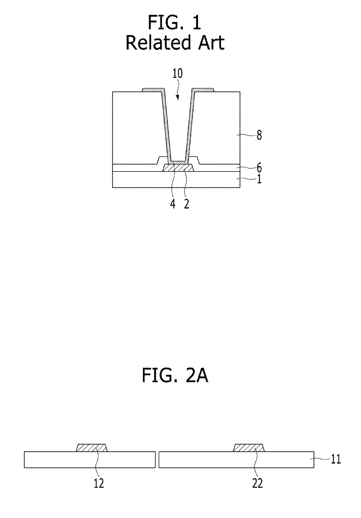
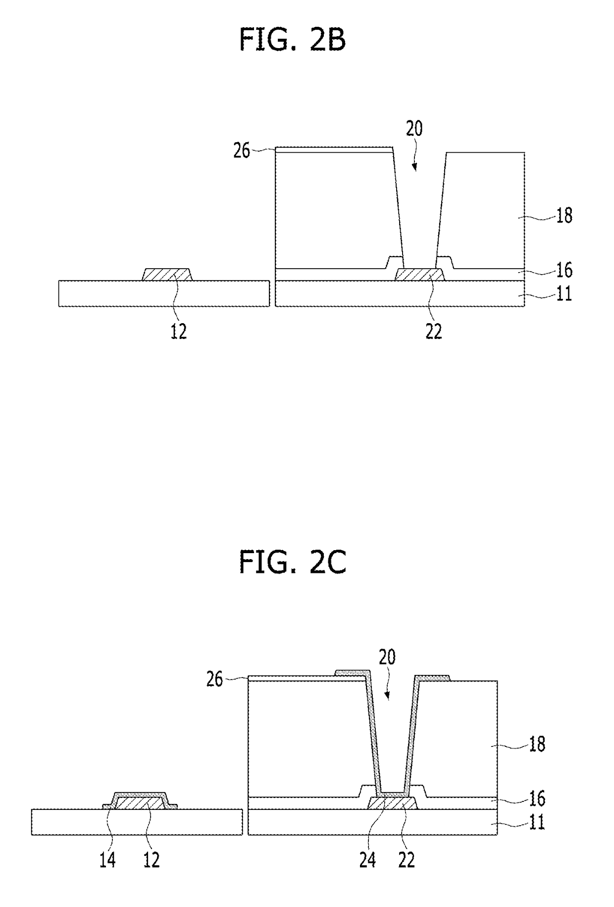
[0027]FIG. 3 is a cross-sectional view of an organic light-emitting display device according to the present disclosure, to which the manufacturing method of FIGS. 2A to 2C is applied.

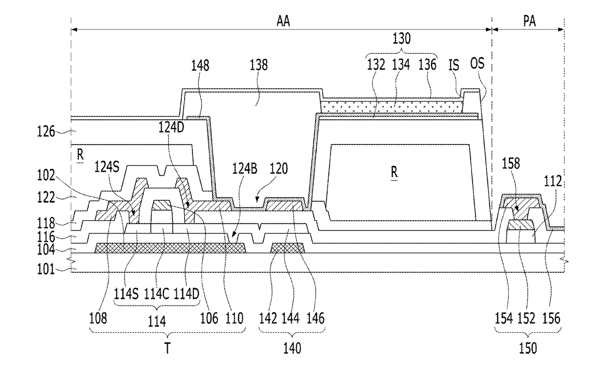
[0028]As illustrated in FIG. 3, the organic light-emitting display device according to the first embodiment of the present disclosure includes an active area AA and a pad area PA. The active area AA will contain a large number of pixels and be relatively large so as to cover most of the device. The pad area PA is usually spaced some distance from the individual pixels; they are not usually directly abutting each other and relative locations in FIG. 3 are not to scale in their distance from each other, the vertical dotted line representing some separation distance.

[0029]On the pad area PA of a substrate 101, a plurality of pads 150 is formed to supply a drive signal to each of a gate line, a data line, and a power line, which are located on the active area AA. Each of the pads 150 includes a first pad el...

second embodiment

[0073]FIG. 8 is a cross-sectional view illustrating an organic light-emitting display device according to the present disclosure.

[0074]The organic light-emitting display device illustrated in FIG. 8 includes the same constituent elements as the organic light-emitting display device illustrated in FIG. 2 except that the pad cover electrode 156 is formed to expose the second pad electrode 154 and the pixel connection electrode 148 is formed to expose the anode electrode 132. Thus, a detailed description related to the same constituent elements will be omitted.

[0075]The pixel connection electrode 148 is formed of an opaque conductive layer having strong corrosion resistance and acid resistance, unlike the anode electrode 132 formed of a transparent conductive layer. For example, the pixel connection electrode 148 is formed of MoTi. Since the pixel connection electrode 148 has a line width similar to that of the bank 138 in the area in which it overlaps the bank 138, the pixel connectio...


PUM


Abstract

Disclosed are a display device and a method of manufacturing the same. In the disclosed display device, a pad cover electrode disposed on a pad area comes into contact with an upper surface and a side surface of a pad electrode since a planarization layer is disposed on an active area excluding the pad area, which may prevent contact failure between the pad cover electrode and a conductive ball. In addition, in the display device, a first electrode, which is connected to a thin film transistor via a pixel connection electrode, is formed via the same mask process as the planarization layer so that it has a line width similar to that of the planarization layer and overlaps the planarization layer, which may simplify a structure and a manufacturing process.

Description

[0001]This application claims the benefit of Korean Patent Application No. 10-2016-0066697, filed on May 30, 2016, which is hereby incorporated by reference as if fully set forth herein.BACKGROUNDTechnical Field[0002]The present disclosure relates to a display device and a method of manufacturing the same, and more particularly, to a display device, which may simplify a structure and a manufacturing process thereof and may also prevent contact failure between a pad cover electrode and a conductive ball, and a method of manufacturing the same.Description of the Related Art[0003]An image display device, which outputs various pieces of information on a screen, is a core technology of the information and communication age, and is being developed in the direction of becoming thinner, lighter, more portable, and having higher performance. Representative examples of such a display device include a liquid crystal display (LCD) device and an organic light-emitting diode (OLED) display device...

Claims


Application Information

Patent Timeline
Patent Type & Authority Applications(United States)
IPC IPC(8): H01L27/32H01L51/56
CPCH01L27/3248H01L27/3258H01L51/56H01L2227/323H01L27/322H01L27/3246H01L27/3262H10K59/123H10K59/122H10K71/00H10K59/38H10K59/124H10K59/1201H01L27/124H01L27/127H01L27/1288H10K59/1213H10K59/131
Inventor NAM, SEUNG-HEEKIM, JEONG-OHBANG, JUNG-HOBEAK, JUNG-SUNLEE, JONG-WON
Owner LG DISPLAY CO LTD
Why Eureka
Try Eureka