Unlock instant, AI-driven research and patent intelligence for your innovation.

Methods, semiconductor devices, and semiconductor systems

Active Publication Date: 2017-12-21
SK HYNIX INC
View PDF0 Cites 2 Cited by
  • Summary
  • Abstract
  • Description
  • Claims
  • Application Information

AI Technical Summary

Benefits of technology

The patent text describes a semiconductor system and device that can shift the storage positions of data based on certain address signals being inputted a certain number of times. This allows for more efficient storage of data and error information. Additionally, the patent describes a method of receiving and outputting data by comparing the number of times certain address signals are inputted with a predetermined number and generating a control signal to shift the data and error information accordingly. The technical effects of this invention include improved data storage efficiency and more efficient data processing.

Problems solved by technology

As the semiconductor devices become more highly integrated with the development of fabrication process techniques, the number of failed memory cells in the tested semiconductor devices has been increasing.
An increase in the number of failed memory cells within the tested semiconductor devices may lead to not only a reduction in the production yield of the semiconductor devices but also difficulty in guaranteeing a large memory capacity for the semiconductor devices.

Method used


Image

  • Methods, semiconductor devices, and semiconductor systems
  • Methods, semiconductor devices, and semiconductor systems
  • Methods, semiconductor devices, and semiconductor systems

Examples


Embodiment Construction

[0015]Various embodiments of the present disclosure will be described hereinafter with reference to the accompanying drawings. However, the embodiments described herein are for illustrative purposes only and are not intended to limit the scope of the present disclosure.

[0016]Various embodiments may be directed to semiconductor devices shifting storage positions of data and a parity signal if a page located at the same position is selected a predetermined number of times or more to store the data and the parity signal, and semiconductor systems including the same.

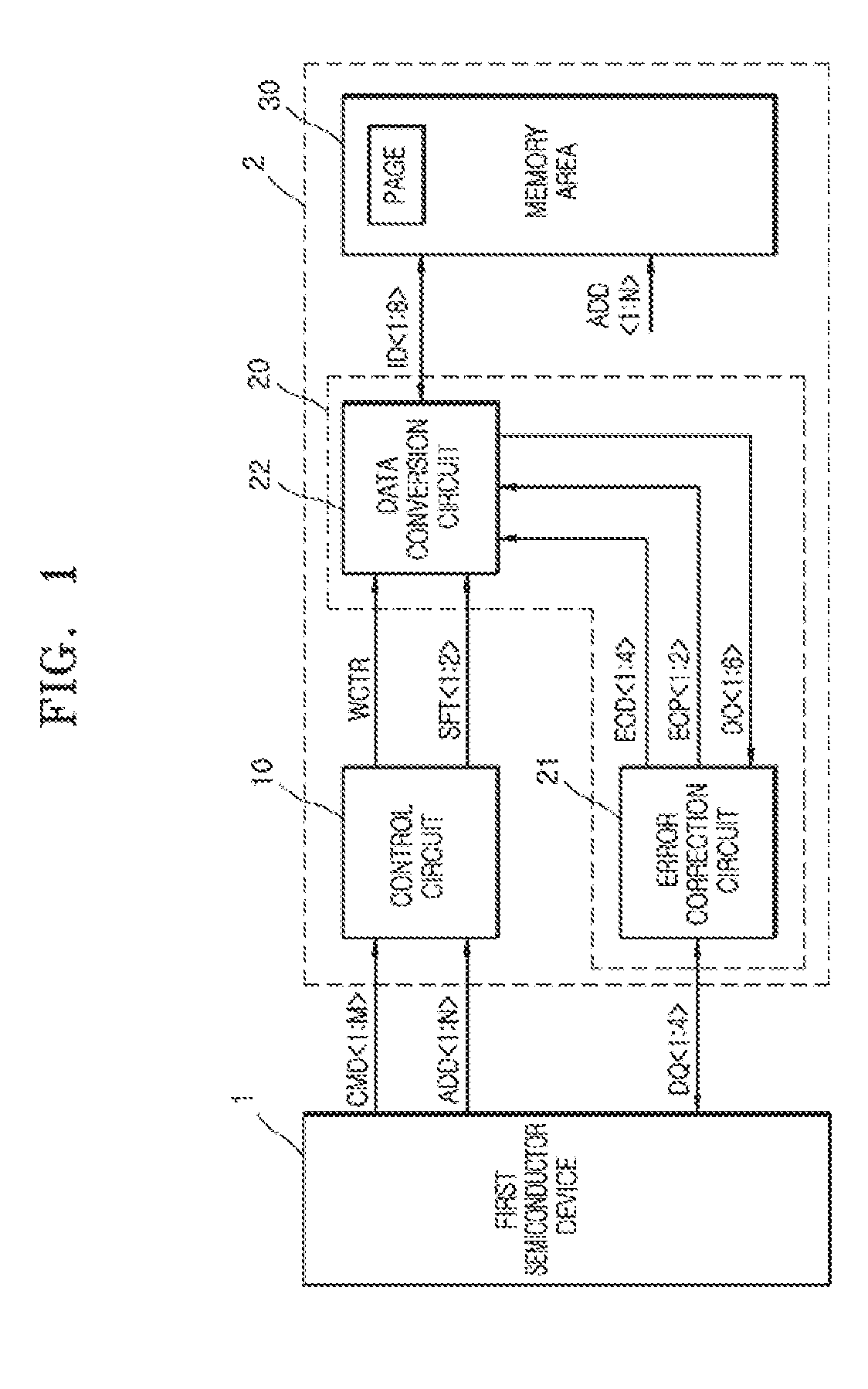
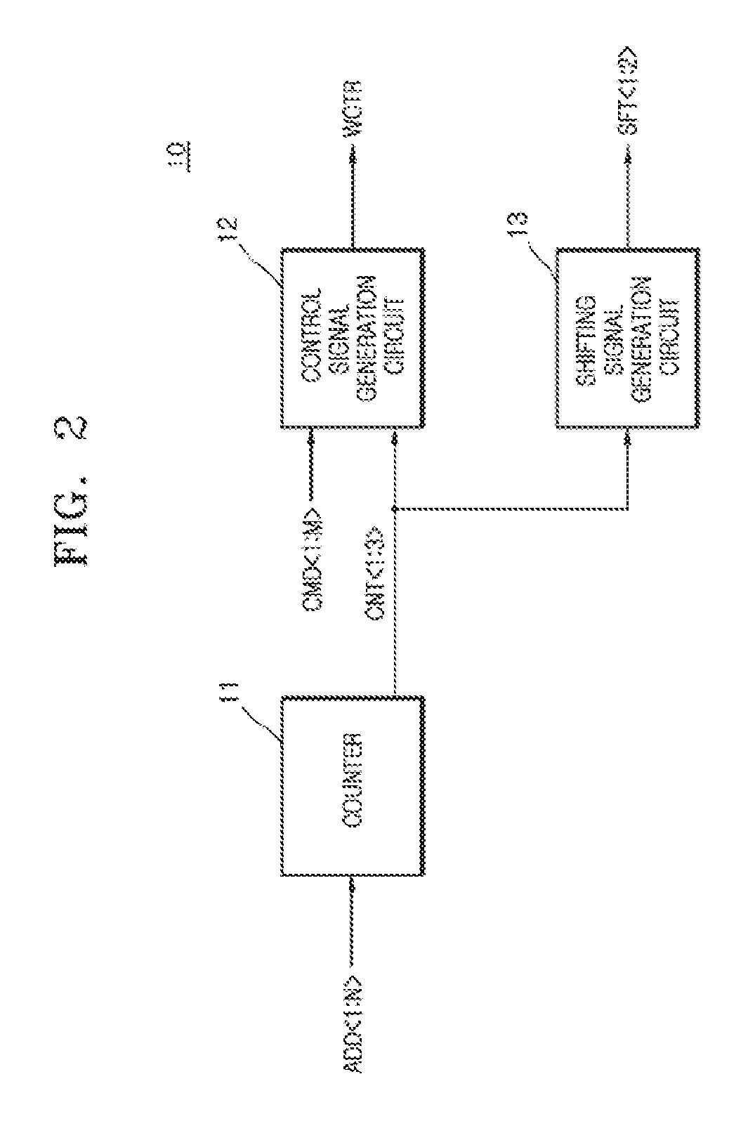
[0017]Referring to FIG. 1, a semiconductor system according to an embodiment of the present disclosure may include a first semiconductor device 1 and a second semiconductor device 2. The second semiconductor device 2 may include a control circuit 10, a data input / output (I / O) circuit 20, and a memory area 30.

[0018]The first semiconductor device 1 may output first to Mth command signals CMD and first to Nth address signals AD...


PUM


Abstract

A semiconductor device may be provided. The semiconductor device may be configured to shift storage positions of data and error information on the data to store the data into shifted storage positions based on the address signals having a certain combination being inputted a predetermined number of times.

Description

CROSS-REFERENCE TO RELATED APPLICATIONS[0001]The present application claims priority under 35 U.S.C 119(a) to Korean Patent Application No. 10-2016-0076051, filed on Jun. 17, 2016, which is incorporated herein by reference in its entirety.BACKGROUND1. Technical Field[0002]Embodiments of the present disclosure may generally relate to semiconductor devices and / or methods for shifting storage positions of data and a parity bit according to the number of times of a write operation and semiconductor systems including the semiconductor devices and / or methods.2. Related Art[0003]Semiconductor devices may be designed and fabricated to include a test mode function for evaluating the operation thereof. That is, various parameters of the semiconductor devices may be measured in a test mode at a wafer level or at a package level. The tested semiconductor devices may be sorted into good chips or failed chips according to the test results.[0004]Each of the semiconductor devices may execute a writ...

Claims


Application Information

Patent Timeline
IPC IPC(8): G11C7/10G06F11/10G11C7/22G06F3/06G11C29/52G11C8/18
CPCG11C7/10G11C7/22G11C8/18G06F3/0679G11C29/52G06F3/0604G06F3/0659G06F11/1068G06F11/1048G11C29/44G11C2029/0411G11C29/42G11C29/022G11C29/18
Inventor JO, SANG GUKIM, DONGGUNKIM, YONG JUHONG, DO-SUN
Owner SK HYNIX INC