Semiconductor substrate and manufacturing method thereof

a technology of semiconductor materials and substrates, applied in the field of substrates, can solve the problems of stress accumulation, material property differences, and influence on epitaxial quality, and achieve the effect of improving the epitaxial quality of iii party nitride semiconductor materials

Active Publication Date: 2018-01-18
GLOBALWAFERS CO LTD
View PDF10 Cites 4 Cited by
  • Summary
  • Abstract
  • Description
  • Claims
  • Application Information

AI Technical Summary

Benefits of technology

[0014]In the invention, defects (especially including, but not limited to, slip lines) can be suppressed from generating in the substrate by manufacturing the injured region inside the periphery region of the plane of the semiconductor substrate. Thereby, the epitaxial quality of the III party nitride semiconductor material can be improved.

Problems solved by technology

In an epitaxial process performed on a heterogeneous substrate, defects may occur due to material property differences.
For example, during a epitaxial process of a III nitride semiconductor material performed on a Si-substrate, epitaxial defects, for example, dislocation, cracks and so on, may occur to an epitaxy layer due to a great stress caused by lattice mismatch and a difference of thermal expansion coefficients, which influences epitaxial quality and is unfavorable for device properties.
Moreover, the difference of thermal expansion coefficients would result in stress accumulation and cause the cracks to occur to an epitaxial film due to a shrinkage difference between the substrate and the epitaxy layer when the epitaxy stops from growing and is cooled down.
For example, the cracks are generated on the epitaxy layer as a surface of the epitaxy layer is influenced by the stress, while slip lines are defects occurring in the substrate because the substrate is deformed by the stress, which results in the occurrence of dislocation or shift on a crystalline plane.
However, the aforementioned conventional methods can only improve the defects occurring to the epitaxy layer, but cannot effectively suppress the defects occurring to the substrate, and the methods disclosed by the related art only disclose forming a stress-relief structure region through an additionally designed buffer layer on the substrate surface or a buffer with a specially processed layer.
Nevertheless, these methods can only suppress the defects from occurring on the surface of the epitaxy layer surface, but cannot suppress the defects or other substrate issues from occurring in the substrate and extending to the epitaxy layer or the epitaxial main plane.
Therefore, as the defects occurring in the substrate cannot be effectively suppressed, the defects may extend toward the epitaxial main plane and further influence the crystal arrangement of the epitaxy layer, which results in reduced quality of the epitaxy layer and is unfavorable for device functions.

Method used


Image

  • Semiconductor substrate and manufacturing method thereof
  • Semiconductor substrate and manufacturing method thereof
  • Semiconductor substrate and manufacturing method thereof

Examples


Embodiment Construction

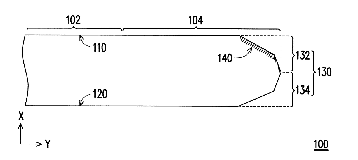
[0026]FIG. 1 is a schematic partial cross-sectional view illustrating a semiconductor substrate according to an embodiment of the invention. Referring to FIG. 1, a semiconductor substrate 100 of the present embodiment includes an epitaxy region 102, a periphery region 104 and an injured region 140. The epitaxy region 102 is located at a central portion of a main plane 110 of the semiconductor substrate 100, the periphery region 104 surrounds the epitaxy region 102, and the injured region 140 is distributed inside the periphery region 104. In another aspect, the semiconductor substrate 100 has the main plane 110, a back surface 120 and a bevel portion 130. The main plane 110 is opposite to the back surface 120, the bevel portion 130 is connected between the main plane 110 and the back surface 120, and the bevel portion 130 is not parallel to the main plane 110. Taking the orientation shown in FIG. 1 for example, the main plane 110 is a plane facing toward a positive X-direction, the ...


PUM


Abstract

A semiconductor substrate and a manufacturing method thereof are provided. The semiconductor substrate has an epitaxy region located at a central portion of a main plane of the semiconductor substrate, a periphery region surrounding the epitaxy region and an injured region distributed inside the periphery region.

Description

CROSS-REFERENCE TO RELATED APPLICATION[0001]This application claims the priority benefits of Taiwan application serial no. 105122010, filed on Jul. 13, 2016, and Taiwan application serial no. 106100952, filed on Jan. 12, 2017. The entirety of each of the above-mentioned patent applications is hereby incorporated by reference herein and made a part of this specification.BACKGROUNDField of the Invention[0002]The invention is directed to a substrate and a manufacturing method thereof and more particularly, to a semiconductor substrate and a manufacturing method thereof.Description of Related Art[0003]In an epitaxial process performed on a heterogeneous substrate, defects may occur due to material property differences. For example, during a epitaxial process of a III nitride semiconductor material performed on a Si-substrate, epitaxial defects, for example, dislocation, cracks and so on, may occur to an epitaxy layer due to a great stress caused by lattice mismatch and a difference of t...

Claims


Application Information

Patent Timeline
Patent Type & Authority Applications(United States)
IPC IPC(8): H01L21/02H01L21/265H01L21/324H01L29/32
CPCH01L21/02021H01L21/324H01L21/265H01L29/32
Inventor FAN, CHUN-ICHUANG, CHIH-YUANSHIH, YING-RUHSU, WEN-CHING
Owner GLOBALWAFERS CO LTD
Why Eureka
Try Eureka