
Hybrid thin film transistor and organic light emitting display device using the same

Active Publication Date: 2018-02-01
LG DISPLAY CO LTD
View PDF4 Cites 45 Cited by
  • Summary
  • Abstract
  • Description
  • Claims
  • Application Information

AI Technical Summary

Benefits of technology

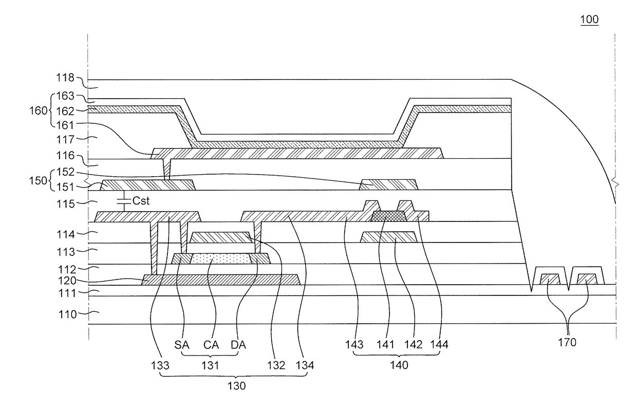
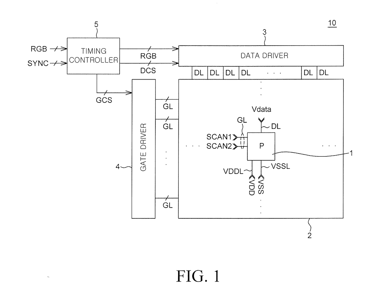
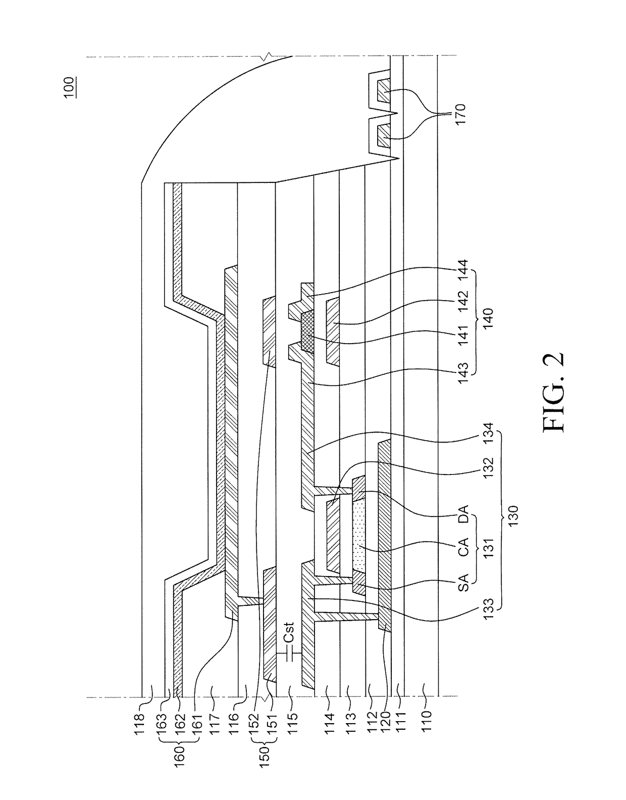
This patent is about a new pixel structure and organic light emitting display device that solves issues with traditional thin film transistors. The device includes a dummy metal pattern on a switching transistor with an oxide semiconductor layer, which improves bias temperature stress and shields external light. This results in a more robust display that can be used for portable and wearable devices while reducing power consumption. The device also has a larger storage capacitor Cst to increase resolution. Overall, this patent provides a technical solution for improving the performance and efficiency of organic light emitting display devices.

Problems solved by technology

The turn-on time of the transistor is related to power consumption of the organic light emitting display device.
However, technologies related to the display devices developed so far have limitations in realizing low power consumption.

Method used


Image

  • Hybrid thin film transistor and organic light emitting display device using the same
  • Hybrid thin film transistor and organic light emitting display device using the same
  • Hybrid thin film transistor and organic light emitting display device using the same

Examples


Embodiment Construction

[0026]Advantages and characteristics of the present disclosure and a method of achieving the advantages and characteristics will be clear by referring to exemplary embodiments described below in detail together with the accompanying drawings. However, the present disclosure is not limited to exemplary embodiment disclosed herein but will be implemented in various forms. The exemplary embodiments are provided by way of example only so that a person of ordinary skilled in the art can fully understand the disclosures of the present disclosure and the scope of the present disclosure. Therefore, the present disclosure will be defined only by the scope of the appended claims.

[0027]The shapes, sizes, ratios, angles, numbers, and the like illustrated in the accompanying drawings for describing the exemplary embodiments of the present disclosure are merely examples, and the present disclosure is not limited thereto.

[0028]Further, in the following description of the present disclosure, a deta...


PUM


Abstract

Different types of thin film transistors are disposed on the same flexible substrate and an organic light emitting display using the same includes a display area and a non-display area; a first buffer layer over an entire surface of the flexible substrate; a driving transistor on the buffer layer in the display area, the driving transistor including a polycrystalline silicon (LIPS) layer, a first gate electrode, a first source electrode, and a first drain electrode; a capacitor electrode on the first source electrode of the driving transistor and forming a storage capacitor together with the first source electrode; a switching transistor in the display area to be spaced apart from the driving transistor; and a dummy electrode on the switching transistor, the dummy electrode formed of the same material as the capacitor electrode, and disposed on the same plane as the capacitor.

Description

CROSS-REFERENCE TO RELATED APPLICATIONS[0001]This application claims the priority of Korean Patent Application No. 10-2016-0095249 filed on Jul. 27, 2016, in the Korean Intellectual Property Office, the disclosure of which is incorporated herein by reference into the present application.BACKGROUNDField[0002]The present disclosure relates to a hybrid thin film transistor in which different types of thin film transistors are disposed on the same flexible substrate and an organic light emitting display device using the same.Description of the Related Art[0003]The demand for display devices is increasing. As such, thin, light, and high resolution flat panel display devices (FPD) have replaced bulky cathode ray tube (CRT) displays.[0004]The flat panel display device can be a light crystal display device (LCD), an organic light emitting display device (OLED), or an electrophoretic display device (ED).[0005]The liquid crystal display device, the organic light emitting display device, and t...

Claims


Application Information

Patent Timeline
IPC IPC(8): H01L27/32H01L51/00
CPCH01L27/3272H01L27/3248H01L27/3265H01L27/3262H01L27/3258H01L51/0097H01L2227/323H01L29/78675H01L29/78633H01L27/1251H01L27/1225H01L29/42384H01L2251/5338H01L29/7869H10K59/1213H10K59/1216H01L29/41733H01L27/1222H01L27/124H01L27/1255Y02E10/549H10K59/88H10K59/126H10K77/111H10K2102/311H10K59/131H10K59/124H10K59/8051H10K59/123G09F9/301H10K59/8052H10K59/873H10K59/1201
Inventor NOH, SOYOUNGJEON, JINCHAESHIN, HYUNSOO
Owner LG DISPLAY CO LTD
Learn More