Organic Light Emitting Diode Display

a light-emitting diode and organic technology, applied in the direction of basic electric elements, electrical apparatus, semiconductor devices, etc., can solve the problems of reducing display quality and limiting flow control, so as to reduce display quality, efficiently control flow, and minimize non-display area width

Active Publication Date: 2018-02-01
LG DISPLAY CO LTD
View PDF2 Cites 30 Cited by
  • Summary
  • Abstract
  • Description
  • Claims
  • Application Information

AI Technical Summary

Benefits of technology

[0020]Such a constraint condition has a limit to implement the organic light emitting diode display having a slim bezel area by minimizing the non-display area of the organic light emitting diode display, and when the upper surface of the protective layer is curved, transmission degrees of the protective layer in the edge area and the center of the organic light emitting diode display may be different from each other, and thus there is a problem in that the display quality is lowered.
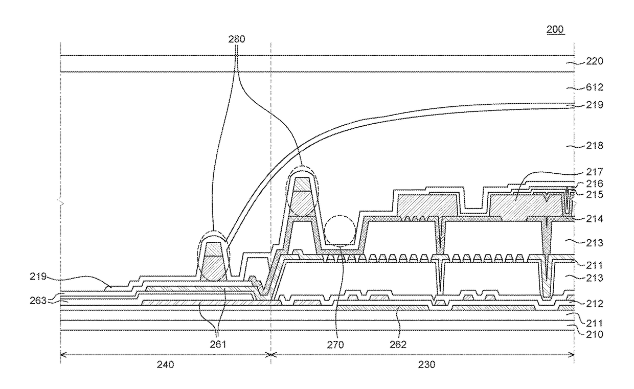
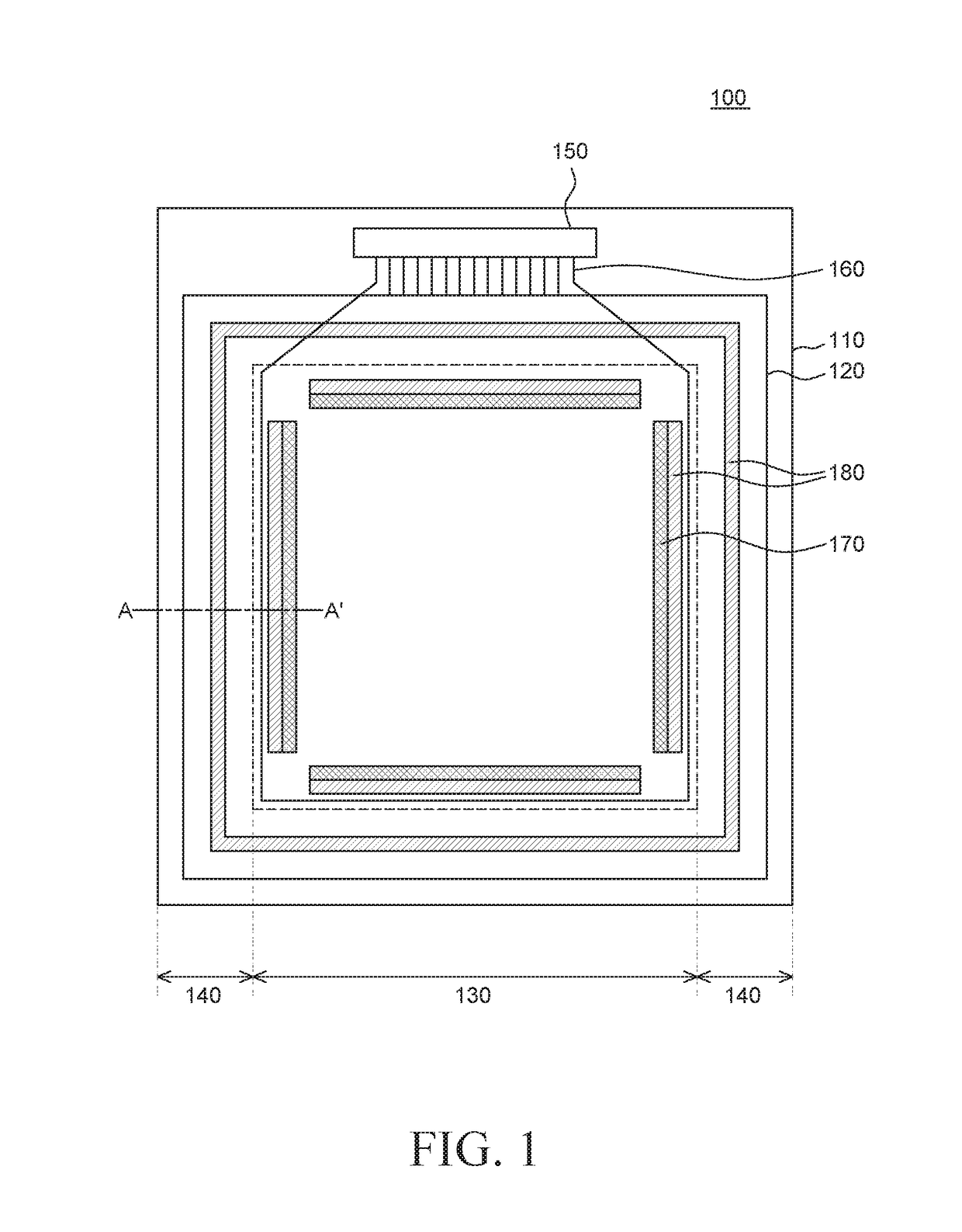
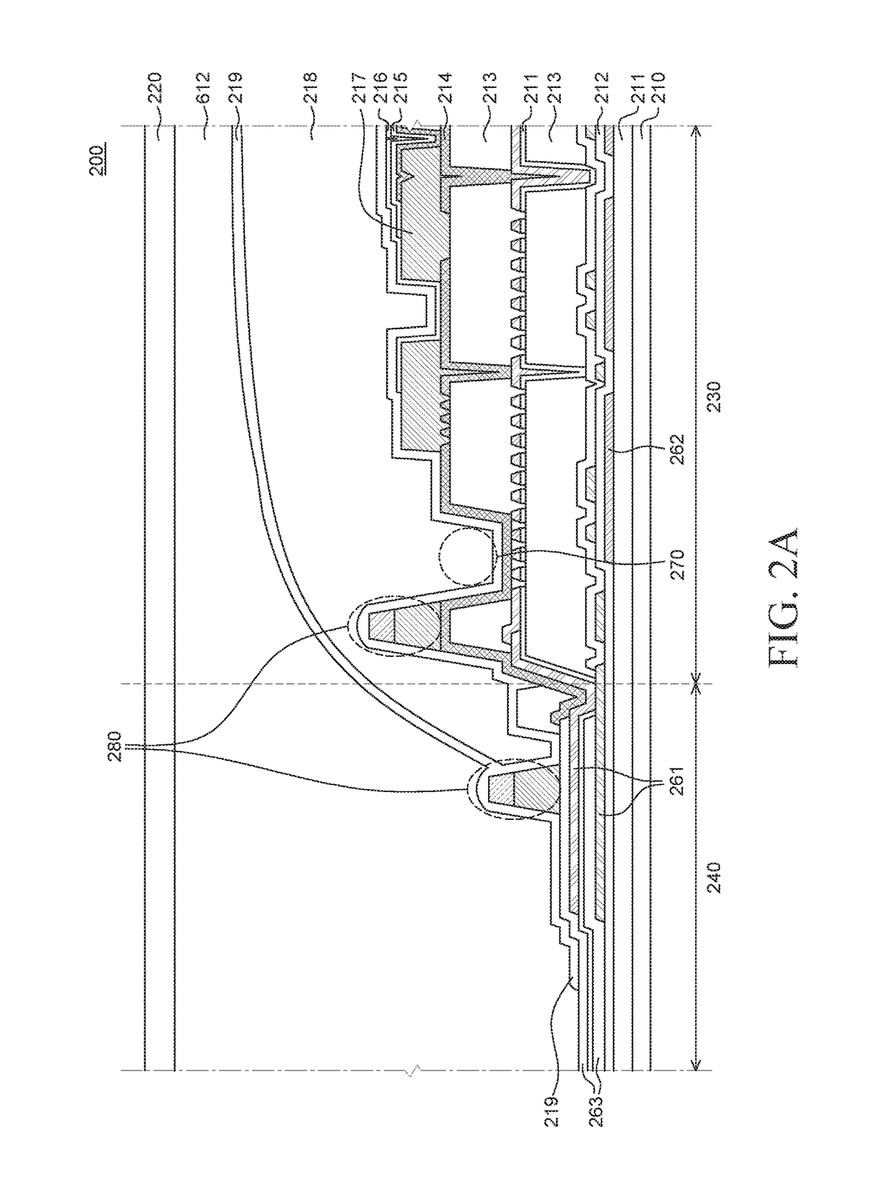
[0021]Therefore, a new structure of the organic light emitting diode display is disclosed. The organic light emitting diode display is capable of minimizing a width of the non-display area by more efficiently controlling a flow of a protective layer formation material when forming the protective layer included in the organic light emitting diode display. Further, a new structure of the organic light emitting diode display is disclosed. The organic light emitting diode display is capable of improving display quality by minimizing a curve of the upper surface of the protective layer while controlling the flow of the protective layer.

Problems solved by technology

However, there may be a limit to control the flow by a dam structure in the non-display area and there is a constraint condition to consider process errors and the like.
Such a constraint condition has a limit to implement the organic light emitting diode display having a slim bezel area by minimizing the non-display area of the organic light emitting diode display, and when the upper surface of the protective layer is curved, transmission degrees of the protective layer in the edge area and the center of the organic light emitting diode display may be different from each other, and thus there is a problem in that the display quality is lowered.

Method used


Image

  • Organic Light Emitting Diode Display
  • Organic Light Emitting Diode Display
  • Organic Light Emitting Diode Display

Examples


Embodiment Construction

[0035]Advantages and features of the present disclosure, and methods for accomplishing the same will be more clearly understood from exemplary embodiments described below with reference to the accompanying drawings. However, the present disclosure is not limited to the following exemplary embodiments but may be implemented in various different forms. The exemplary embodiments are provided only to complete disclosure of the present disclosure and to fully provide a person having ordinary skill in the art to which the present disclosure pertains with the category of the disclosure, and the present disclosure will be defined by the appended claims.

[0036]The shapes, sizes, ratios, angles, numbers, and the like illustrated in the accompanying drawings for describing the embodiments of the present disclosure are merely examples, and the present disclosure is not limited thereto. Like reference numerals generally denote like elements throughout the present specification. Further, in the fo...


PUM


Abstract

An organic light emitting diode display is disclosed in which a flow control pattern of an organic protective layer is disposed to implement a thin bezel. In an active area and a bezel area defined on a substrate, the flow control pattern disposed reduces the flow of a protective layer so as to minimize area size of the bezel area.

Description

CROSS-REFERENCE TO RELATED APPLICATIONS[0001]This application claims the priority of Korean Patent Application No. 10-2016-0097214 filed on Jul. 29, 2016 and Korean Patent Application No. 10-2016-0143250 filed on Oct. 31, 2016 in the Korean Intellectual Property Office, each of which is hereby incorporated by reference in its entirety.BACKGROUNDField[0002]The present disclosure relates to an organic light emitting diode display and more particularly, to an organic light emitting diode display including a flow control pattern configured to more efficiently control a flow of an adhesive layer disposed on an organic light emitting element or a protective layer made of an organic material.Description of the Related Art[0003]Recent display devices which can display various information and interact with a user who views the corresponding information have various sizes, various shapes, and various functions.[0004]The display devices include a liquid crystal display device (LCD), a plasma d...

Claims


Application Information

Patent Timeline
Patent Type & Authority Applications(United States)
IPC IPC(8): H01L51/52H01L27/32
CPCH01L51/525H01L27/3258H01L27/3246H01L51/5253H10K59/12H10K50/00H10K50/84H10K59/122H10K59/124H10K50/844H10K50/8428
Inventor KIM, JINHWANKIM, WOOCHANUM, HYUNCHUL
Owner LG DISPLAY CO LTD
Why Eureka
Try Eureka