Manufacturing method of light emitting device package

Active Publication Date: 2018-02-08
SUZHOU LEKIN SEMICON CO LTD
View PDF1 Cites 0 Cited by
  • Summary
  • Abstract
  • Description
  • Claims
  • Application Information

AI Technical Summary

Benefits of technology

[0013]In a light emitting device package according to an embodiment, a molding part including a CYTOP transmitting at least 90% of an ultraviolet wavelength is formed on a light emitting device, and thus not only light efficiency can be enhanced but also reliability of the product can be improved with high durability.
[0014]In the light emitting device package according to the embodiment, the molding part including the CYTOP is formed on the light emitting device, thereby preventing the reliability degradation by adhesive damage of a general light emitting device package including a quartz film and an adhesive and thus a yield can be improved.
[0015]In addition, in the light emitting device package according to the embodiment, an expensi

Problems solved by technology

However, in the light emitting device having a general ultraviolet wavelength, there is a problem that poor bonding between the body and the qua

Method used


Image

  • Manufacturing method of light emitting device package
  • Manufacturing method of light emitting device package
  • Manufacturing method of light emitting device package

Examples


Example

MODES OF THE INVENTION

[0026]Hereinafter, a light emitting device package according to an embodiment will be described with reference to the accompanying drawings. In the description of embodiments, it will be understood that when a layer (or film), region, pattern or structure is referred to as being “on” or “under” another layer (or film), region, pattern or structure, the terminology of “on” and “under” comprises both the meanings of “directly” or “by interposing another layer (indirectly)”. Further, the reference about “on” and “under” each layer will be made on the basis of drawings.

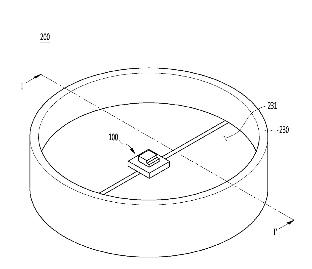
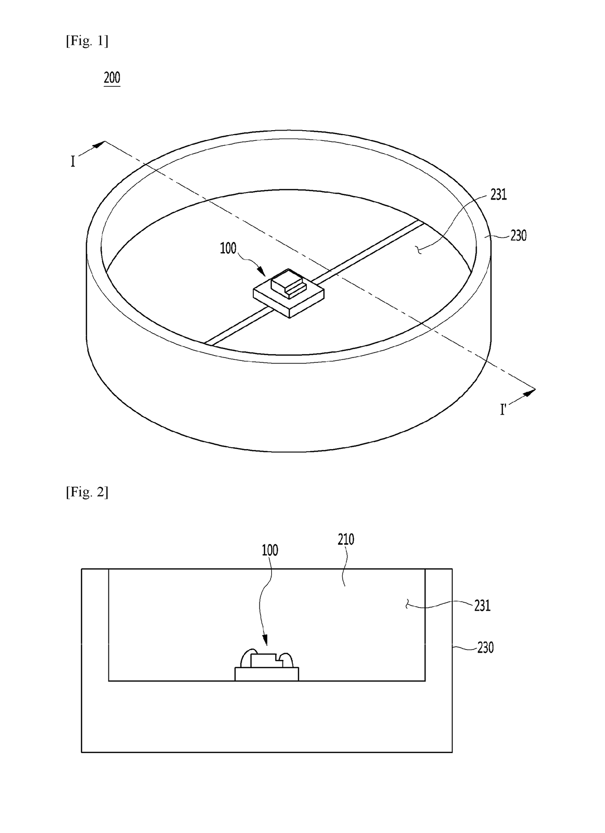
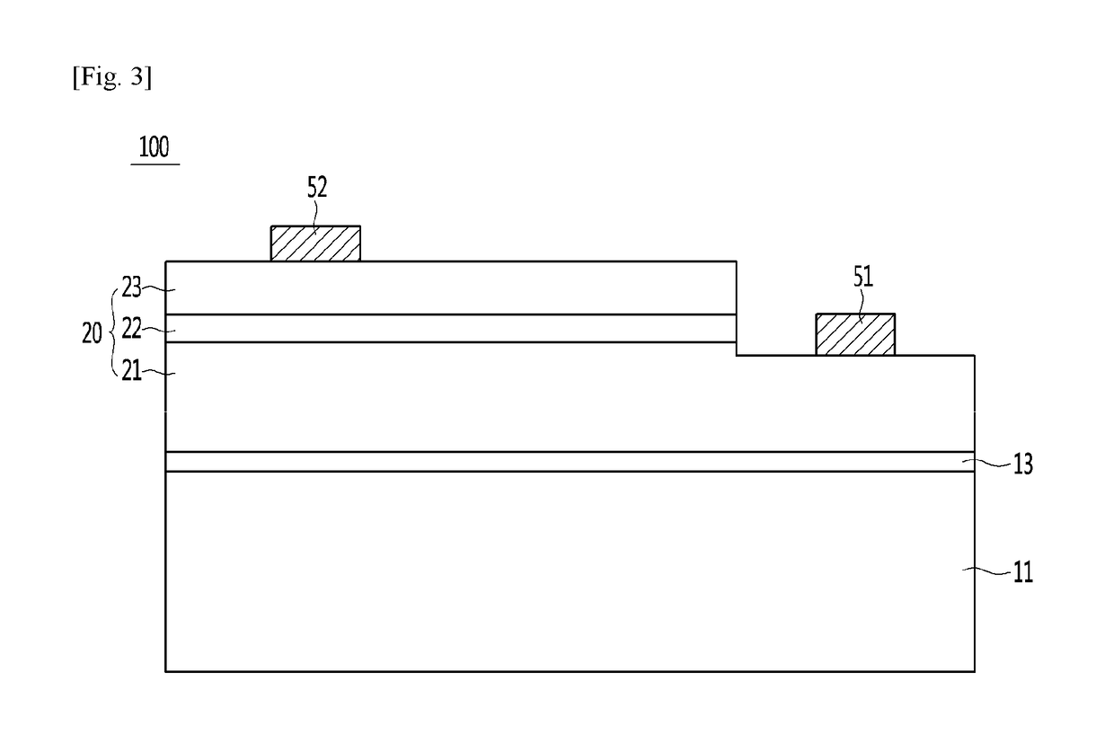
[0027]FIG. 1 is a perspective view illustrating a light emitting device package according to an embodiment, FIG. 2 is a cross-sectional view illustrating the light emitting device package taken along line I-I′ of FIG. 1, and FIG. 3 is a cross-sectional view illustrating a light emitting device of FIG. 1 according to the embodiment.

[0028]Referring to FIGS. 1 to 3, a light emitting device package 200 a...


PUM


Abstract

An embodiment relates to a light emitting device package and a manufacturing method of the light emitting device package. The light emitting device package according to an embodiment may include a body having a top opened cavity, a light emitting device mounted on an inner bottom surface of the cavity, and a molding part accommodated in the cavity to protect the light emitting device, and the molding part may include a CYTOP, and thus not only light efficiency can be enhanced but also the reliability of the product can be improved with high durability.

Description

TECHNICAL FIELD[0001]The embodiment relates to a light emitting device package, a manufacturing method of the light emitting device package, and a light source unit.BACKGROUND ART[0002]A light emitting device is a p-n junction diode having characteristics of converting electric energy into light energy, may be configured with a compound semiconductor of Group III and Group V elements or the like of the periodic table and may represent various colors by adjusting a composition ratio of a compound semiconductor.[0003]GaN-based light emitting device (LED) has been used for various applications such as a natural color LED display device, a LED traffic signal, and white LED. Recently, luminous efficiency of a high-efficiency white LED is more excellent than that of a conventional fluorescent lamp, and is expected to replace a fluorescent lamp in a general illumination field.[0004]A light emitting device having a general ultraviolet wavelength mounts an ultraviolet light emitting device i...

Claims


Application Information

Patent Timeline
IPC IPC(8): H01L33/00H01L33/52H01L33/50
CPCH01L33/005H01L33/502H01L33/52H01L2933/0041H01L2933/005H01L33/56
Inventor KIM, MYUNG HEEHONG, JUNG YEOP
Owner SUZHOU LEKIN SEMICON CO LTD
Why Eureka
Try Eureka