Inverter circuit and power conversion device

a technology of inverter circuit and power conversion device, which is applied in the direction of dc-ac conversion without reverse, efficient power electronics conversion, emergency protective circuit arrangement, etc., can solve the problems of large parasitic capacitance, poor reverse recovery characteristic of built-in diodes, and damage to each device, etc., to suppress abnormality generation, excellent effect, and suppress overvoltag

Active Publication Date: 2018-02-08
ORMON CORP
View PDF7 Cites 9 Cited by
  • Summary
  • Abstract
  • Description
  • Claims
  • Application Information

AI Technical Summary

Benefits of technology

[0022]One or more aspects may include a switching element, and a clamp element connected to the switching element, as a short circuit part configured to short-circuit output from a full-bridge inverter. Consequently, the clamp element can suppress an overvoltage applied to the switching element, and therefore excellent effects capable of suppressing generation of abnormality such as damage of the switching element, and the like is exhibited.

Problems solved by technology

However, while the SJ-MOSFET is expected as a high efficient device which is relatively a low cost, and has low on-resistance, the SJ-MOSFET has a problem that parasitic capacitance is large, and a reverse recovery characteristic of a built-in diode is poor.
At this time, when the parasitic capacitance of the switching element Q6 is large, each device may be damaged by a surge voltage resulting from resonance.

Method used


Image

  • Inverter circuit and power conversion device
  • Inverter circuit and power conversion device
  • Inverter circuit and power conversion device

Examples


embodiment 1

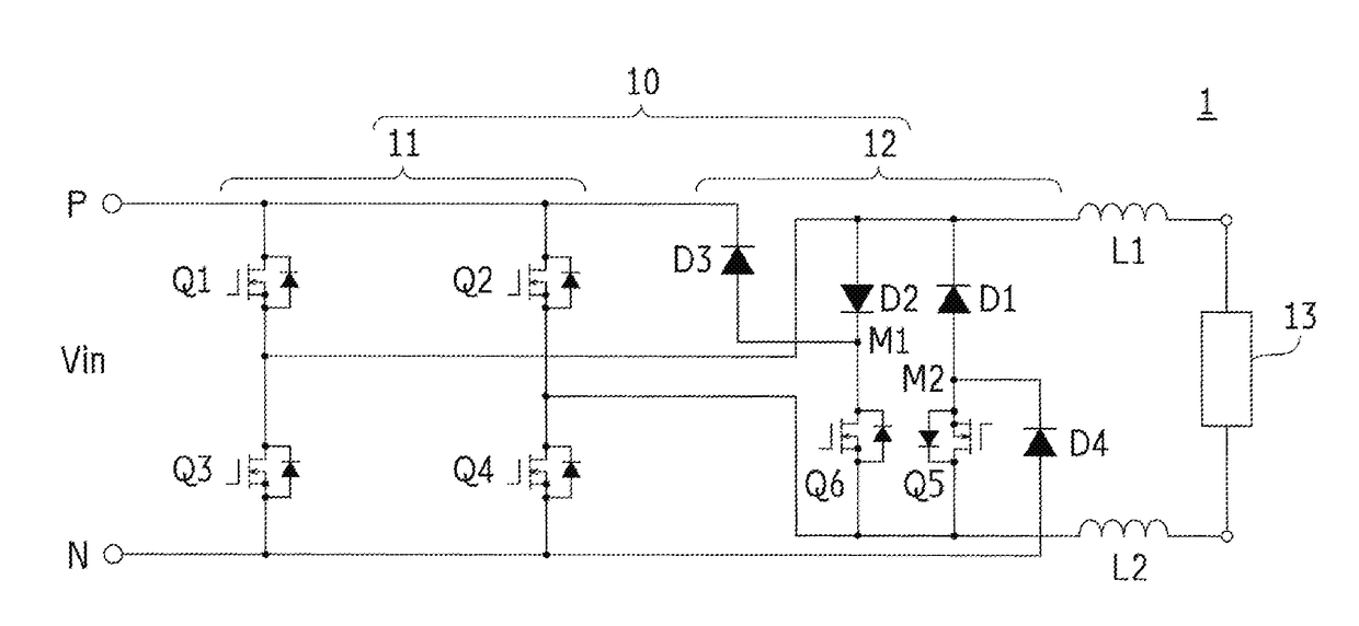
[0043]FIG. 3A and FIG. 3B each are a circuit diagram illustrating an example of a power conversion device including an inverter circuit. FIG. 3A illustrates a power conversion device 1 including an inverter circuit 10 of Embodiment 1, and FIG. 3B illustrates a power conversion device including a conventional inverter circuit for comparison. The power conversion device 1 illustrated in FIG. 3A is used in a system such as a solar power generation system, and includes the inverter circuit 10 that receives a DC voltage output from a power source such as a solar battery (not illustrated) in an input part to convert the received DC voltage to an AC voltage, inductors L1, L2, and outputs the AC voltage converted by the inverter circuit 10 from an output part to an electric power load 13 through the inductors L1, L2. The DC voltage received by the power conversion device 1 that includes the inverter circuit 10 is converted to a suitable voltage by a converter (not illustrated) such as a DC-...

embodiment 2

[0052]FIG. 5A and FIG. 5B each are a circuit diagram illustrating an example of a power conversion device including an inverter circuit. FIG. 5A illustrates a power conversion device 2 including an inverter circuit 20 of Embodiment 2, and FIG. 5B illustrates a power conversion device including a conventional inverter circuit for comparison. The power conversion device 2 illustrated in FIG. 5A includes the inverter circuit 20, and inductors L1, L2, and outputs an AC voltage converted by the inverter circuit 20 to an electric power load 23 through the inductors L1, L2.

[0053]The inverter circuit 20 illustrated in FIG. 5A includes a full-bridge inverter 21, and a short circuit part 22. Configurations of the power conversion device 2 and the inverter circuit 20 of Embodiment 2 other than the short circuit part 22 are similar to the configurations of the power conversion device and the inverter circuit of Embodiment 1, and therefore for the similar configurations, Embodiment 1 should be r...

experiment 1

[0058]Now, a result of an experiment for simulatively applying a surge voltage in the inverter circuits according to the above embodiments will be described as a simulation test. As the simulation test according to Experiment 1, a phenomenon that occurred in a case where voltage input to the inverter circuit 20 described with reference to FIG. 5A started was confirmed. Experiment 1 was performed on condition of input voltage (DC): 370 Vdc, output voltage (AC): 202 Vac, rated power output: 5.5 kw, switching frequency: 20 kHz, inductors L1, L2: 700 μH. For comparison, the experiment was performed for the conventional inverter circuit illustrated in FIG. 5B along with the inverter circuit 20 of Embodiment 2 illustrated in FIG. 5A on the same condition.

[0059]FIG. 6A and FIG. 6B each are a graph illustrating an experimental result for the inverter circuit. FIG. 6A and FIG. 6B each are a graph illustrating a change with time of a drain-source voltage Vds6 of the switching element Q6 in a ...


PUM


Abstract

An inverter circuit provided in a power conversion device includes a full-bridge inverter, and a short circuit part. The short circuit part includes switching elements and clamp elements connected to the switching elements. The clamp elements suppress application of an excessive voltage such as a surge voltage to the switching elements.

Description

CROSS REFERENCE TO RELATED APPLICATIONS[0001]This application is a continuation application of International Application No. PCT / JP2016 / 057181, filed on Mar. 8, 2016, which claims priority based on the Article 8 of Patent Cooperation Treaty from prior Japanese Patent Application No. 2015-131464, filed on Jun. 30, 2015, the entire contents of which are incorporated herein by reference.TECHNICAL FIELD[0002]The disclosure relates to an inverter circuit including a short circuit part configured to short-circuit output from a full-bridge inverter, and a power conversion device.BACKGROUND ART[0003]For example, in a power conversion device such as an inverter that converts, into an AD, a DC output obtained by power generation by a solar battery, a HERIC CIRCUIT obtained by combining a full-bridge inverter with a switching element that short-circuits is used (for example, refer to Patent Document 1).[0004]As a switching element used in a device such as a power conversion device, an SJ-MOSFE...

Claims


Application Information

Patent Timeline
Patent Type & Authority Applications(United States)
IPC IPC(8): H02M7/5387H02M7/797H02J3/38
CPCH02M7/5387H02J3/383H02M7/797H02M2001/123Y02E10/56Y02B70/10H02M1/342H02M1/34H02H7/122H02M7/48H02M1/0051H02M1/123
Inventor NISHIKAWA, TAKEOOKADA, WATARUTAWARAGI, TAKAYOSHIIWAI, SATOSHI
Owner ORMON CORP
Why Eureka
Try Eureka