
Multilayer ceramic electronic component

a technology of electronic components and ceramics, applied in the direction of fixed capacitors, stacked capacitors, fixed capacitor details, etc., can solve the problems of increased equivalent series resistance, multilayer body cracks, and difficulty in sufficiently releasing stress, and achieve the effect of convenient mounting

Active Publication Date: 2018-05-31
MURATA MFG CO LTD
View PDF7 Cites 28 Cited by
  • Summary
  • Abstract
  • Description
  • Claims
  • Application Information

AI Technical Summary

Benefits of technology

This patent describes a new way to make electronic components that have reduced stress and cracks. The approach involves using layers of conductive resin to release stress and prevent damage to the component. The conductive resin layers cover the underlying electrode layers and have a specific pattern to minimize stress and improve solder bonding. This design significantly reduces the chances of failure and improves the performance of the electronic components.

Problems solved by technology

However, even in the structure disclosed in Japanese Unexamined Patent Application Publication No. 11-162771, when the stress due to an impact of dropping or the flexural stress generated by thermal expansion and contraction of a mounting substrate, the thermal expansion and contraction being caused by heat cycles, is extremely increased, it is difficult to sufficiently release the stress, and the multilayer body cracks in some cases.
Furthermore, the design in which an epoxy-based thermosetting resin layer is located between an underlying electrode layer and a Ni plating layer as in Japanese Unexamined Patent Application Publication No. 11-162771 may be disadvantageous in that the contact resistance between the epoxy-based thermosetting resin layer and the Ni plating layer increases, resulting in an increase in the equivalent series resistance (ESR).

Method used


Image

  • Multilayer ceramic electronic component
  • Multilayer ceramic electronic component
  • Multilayer ceramic electronic component

Examples


Embodiment Construction

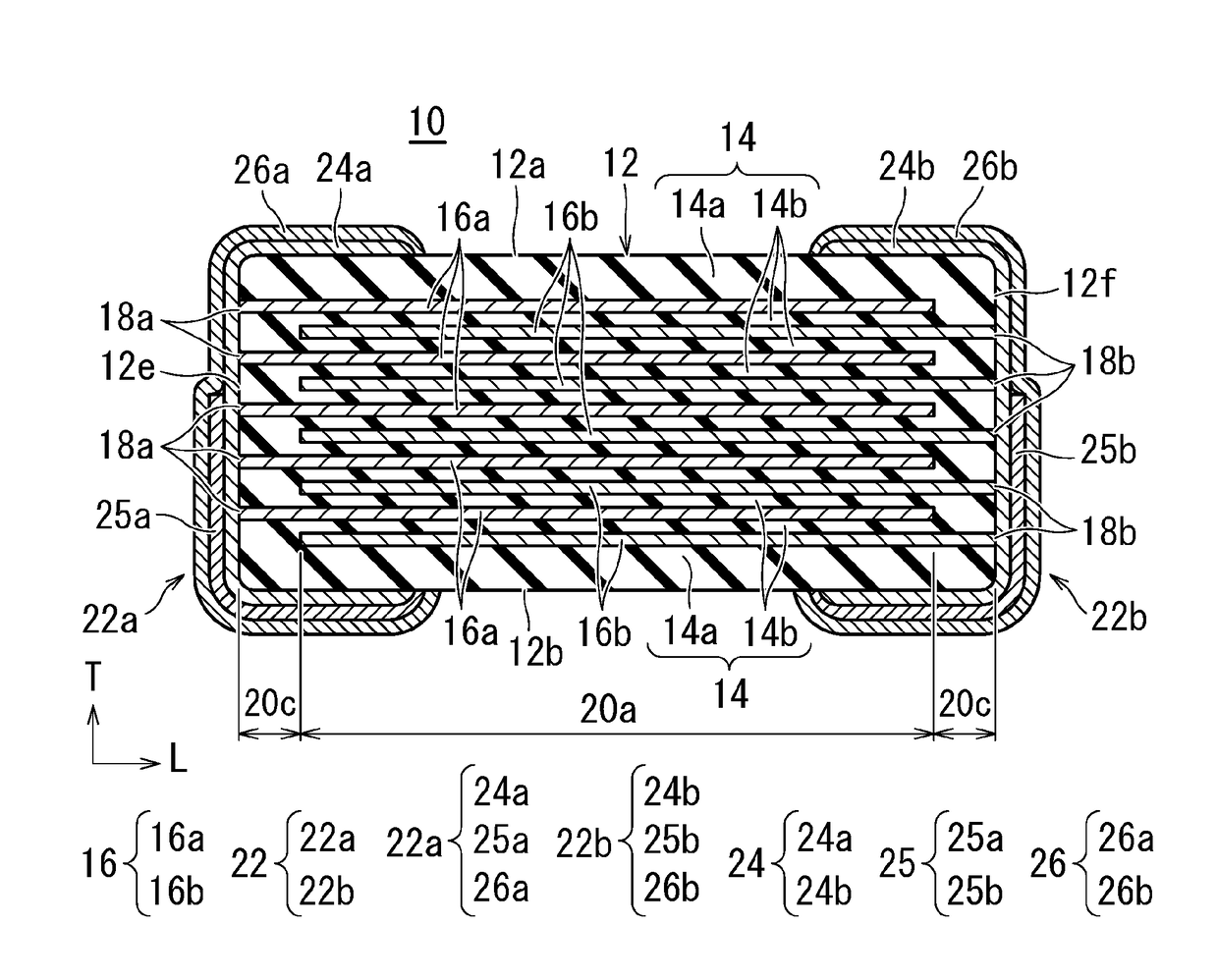
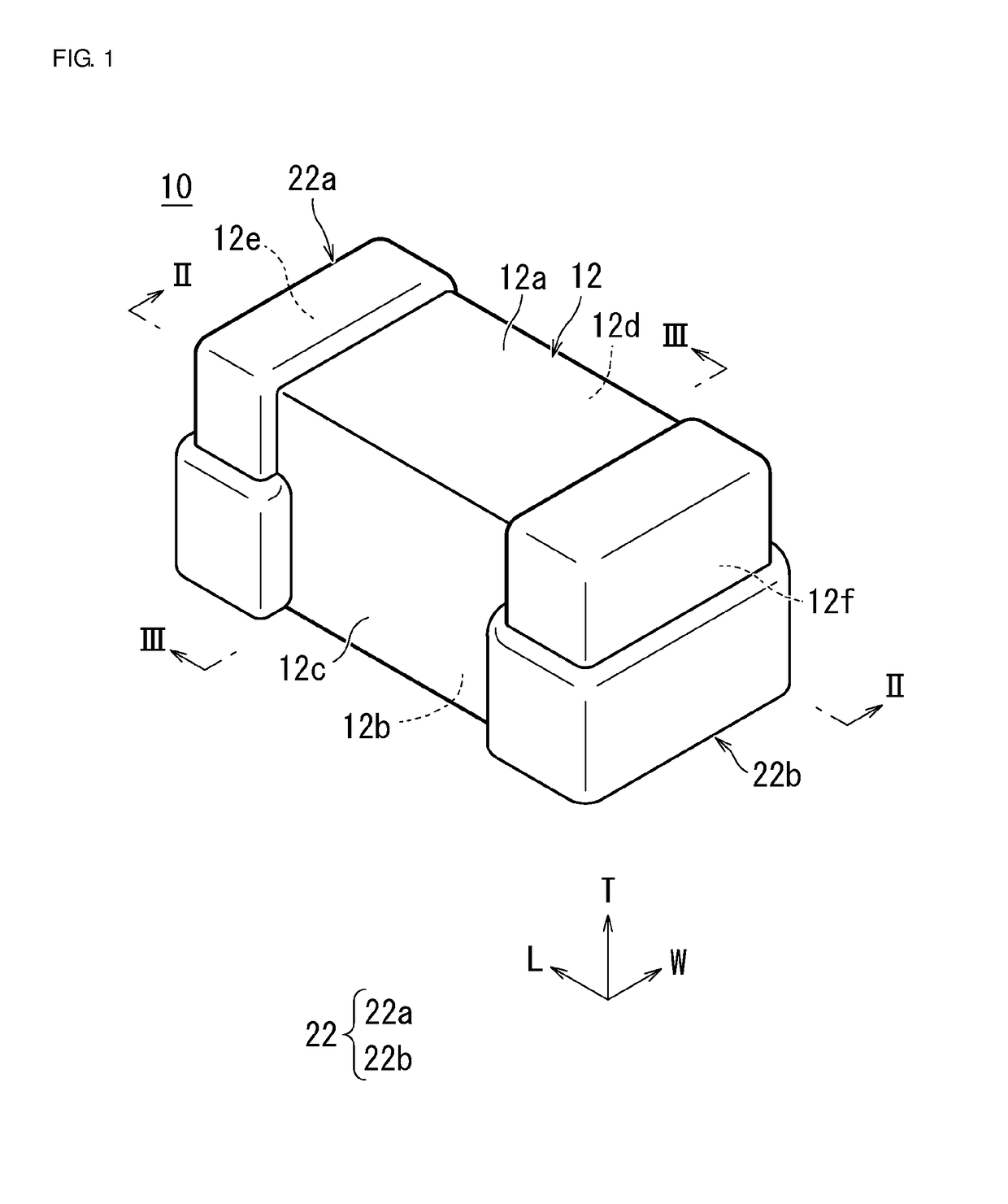
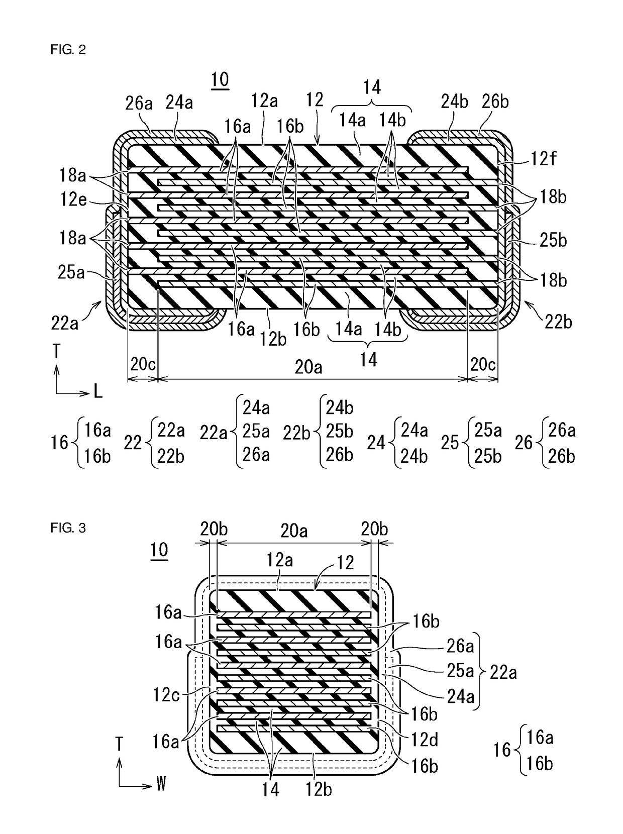
[0035]Preferred embodiments of the present invention will be described below with reference to the drawings.

[0036]It is to be noted that the following preferred embodiments represent examples of the present invention for merely illustrative purposes, and that the present invention is not limited to matters disclosed in the following preferred embodiments. The matters disclosed in the different preferred embodiments are able to be combined with each other in practical applications, and modified preferred embodiments in those cases are also included in the scope of the present invention. The drawings serve to assist understanding of the preferred embodiments, and they are not always exactly drawn in a strict sense. In some cases, for instance, dimension ratios between constituent elements themselves or dimension ratios of distances between elements or features, which are shown in the drawings, are not in match with the dimension ratios described in the Description. Furthermore, some o...


PUM

PropertyMeasurementUnit
thicknessaaaaaaaaaa
thicknessaaaaaaaaaa
thicknessaaaaaaaaaa

Abstract

A multilayer ceramic electronic component includes a multilayer body that includes a second main surface defining and functioning as a mounting surface. Outer electrodes include underlying electrode layers including a conductive metal and a glass component and conductive resin layers including a thermosetting resin and a metal component. The underlying electrode layers extend from first and second end surfaces onto at least the second main surface. The conductive resin layers extend onto the underlying electrode layers provided on the second main surface, portions of the second main surface, and portions of the underlying electrode layers provided on the first end surface and the second end surface and cover portions of the first and second end surfaces, the portions including areas corresponding to about 9% or more and about 82% or less of areas of the first and the second end surfaces.

Description

CROSS REFERENCE TO RELATED APPLICATIONS[0001]This application claims the benefit of priority to Japanese Patent Application No. 2016-230112 filed on Nov. 28, 2016. The entire contents of this application are hereby incorporated herein by reference.BACKGROUND OF THE INVENTION1. Field of the Invention[0002]The present invention relates to a multilayer ceramic electronic component that includes a multilayer body including a plurality of dielectric layers and a plurality of inner electrode layers, the dielectric layers and the inner electrode layers being laminated, and outer electrodes provided on end surfaces of the multilayer body to be electrically connected to the inner electrode layers.2. Description of the Related Art[0003]In recent years, ceramic electronic components, such as, multilayer ceramic capacitors, have been used in more severe environments than in the past.[0004]For example, multilayer ceramic capacitors included in mobile devices such as, cellular phones and portable...

Claims


Application Information

Patent Timeline
Patent Type & Authority Applications(United States)
IPC IPC(8): H01G4/12H01G4/232H01G4/008H01G4/30H01G2/06
CPCH01G4/12H01G4/2325H01G4/008H01G4/30H01G2/065H01G4/232
Inventor YAMADA, MAYUMI
Owner MURATA MFG CO LTD
Learn More