Semiconductor device and fabrication method thereof

a technology of semiconductors and semiconductors, applied in the direction of semiconductor devices, basic electric elements, electrical equipment, etc., can solve problems such as serious leakage currents

Active Publication Date: 2018-06-07
SEMICON MFG INT (SHANGHAI) CORP +1
View PDF2 Cites 2 Cited by
  • Summary
  • Abstract
  • Description
  • Claims
  • Application Information

AI Technical Summary

Benefits of technology

[0007]One aspect of the present disclosure provides a method for fabricating a semiconductor device. The method includes providing a substrate; forming a gate structure film on the substrate; forming a patterned mask structure on the gate structure film, where the patterned mask structure includes a first mask layer at least including a...

Problems solved by technology

A conventional planar MOS transistor has weak control capability on the channel current...

Method used


Image

  • Semiconductor device and fabrication method thereof
  • Semiconductor device and fabrication method thereof
  • Semiconductor device and fabrication method thereof

Examples


Embodiment Construction

[0014]The objects, features and advantages of the present disclosure can be understood by those skilled in the art through the exemplary embodiments of the present disclosure, and can be further described in detail with reference to the accompanying drawings.

[0015]FIGS. 1-4 illustrate a fabrication method of a semiconductor device.

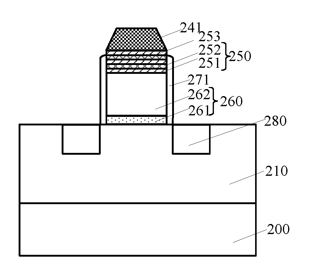
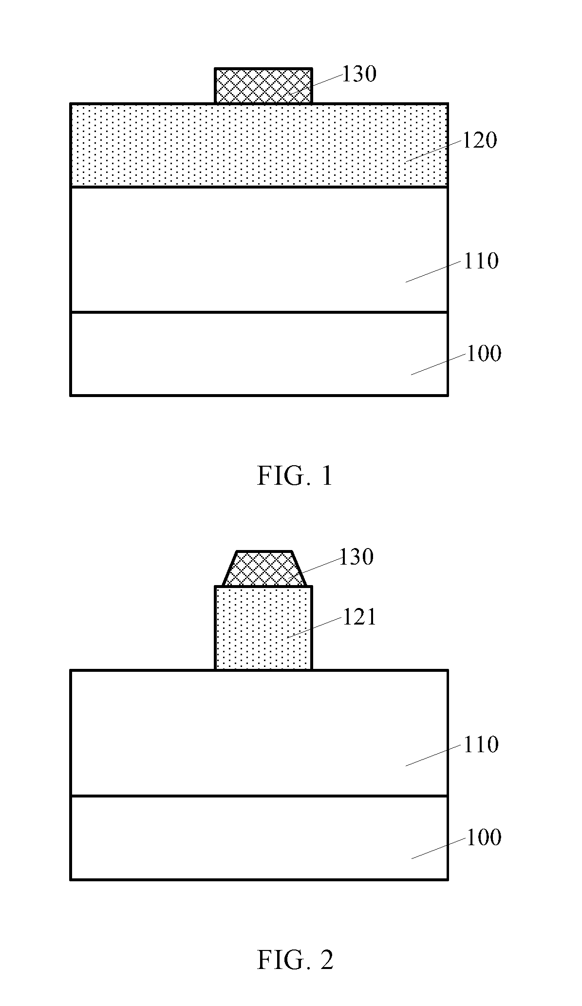
[0016]As shown in FIG. 1, the fabrication method may begin with: providing a semiconductor substrate 100 having a fin 110 on the semiconductor substrate 100, forming a dummy gate structure film 120 on the semiconductor substrate 100 to cover the fin 110, and forming a patterned mask layer 130 on the dummy gate structure film 120.

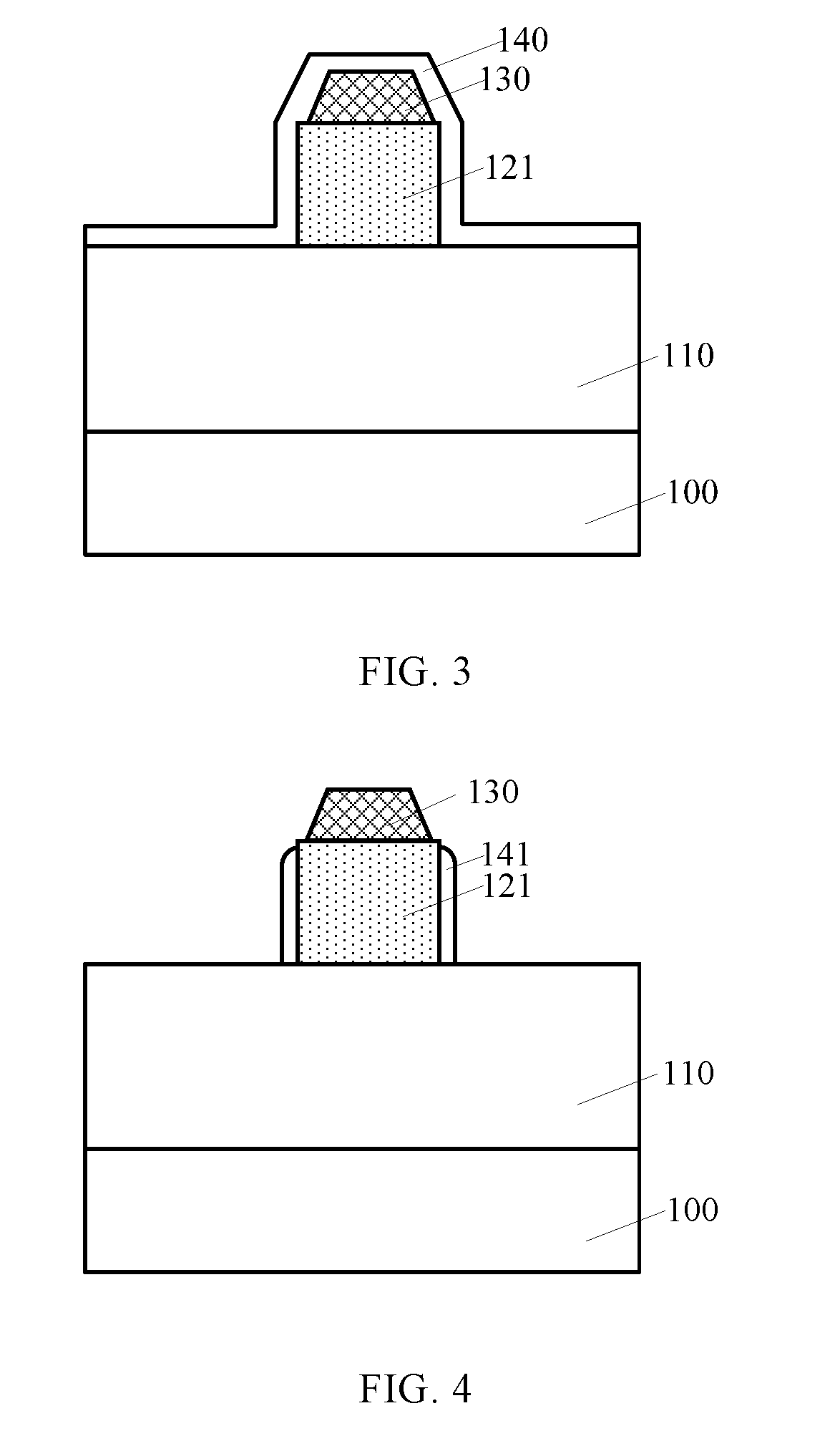
[0017]As shown in FIG. 2, the fabrication method may further include: etching the dummy gate structure film 120 (referring to FIG. 1) by using the mask layer 130 as an etch mask to form a dummy gate structure 121 across the fin 110.

[0018]As shown in FIG. 3, the fabrication method may further include: forming a spacer film 140 cover...


PUM


Abstract

A semiconductor device and a fabrication method are provided. The method includes providing a substrate; forming a gate structure film on the substrate; forming a patterned mask structure on the gate structure film, where the patterned mask structure includes a first mask layer at least including a first material layer and a second mask layer on the first mask layer; forming a gate structure on the substrate by etching the gate structure film using the patterned mask structure as an etch mask, where the first material layer has an etching rate smaller than the second mask layer; and forming a spacer at least on a sidewall of the gate structure.

Description

CROSS-REFERENCES TO RELATED APPLICATIONS[0001]This application claims priority of Chinese Patent Application No. 201611110266.7, filed on Dec. 2, 2016, the entire contents of which are hereby incorporated by reference.FIELD OF THE INVENTION[0002]The present disclosure generally relates to the field of semiconductor manufacturing and, more particularly, relates to a semiconductor device and a fabrication method thereof.BACKGROUND[0003]A metal-oxide-semiconductor (MOS) transistor is one of the most important elements in modern integrated circuits. The basic structure of a MOS transistor includes a semiconductor substrate; a gate structure on the semiconductor substrate. The gate structure includes a gate dielectric layer on the surface of the semiconductor substrate and a gate electrode layer on the surface of the gate dielectric layer; and doped source and drain regions in the semiconductor substrate on both sides of the gate structure.[0004]A conventional planar MOS transistor has w...

Claims


Application Information

Patent Timeline
IPC IPC(8): H01L29/66H01L21/3213H01L21/033H01L29/78
CPCH01L29/66545H01L21/32139H01L21/32133H01L21/0332H01L29/66636H01L29/66795H01L29/7848H01L29/7851H01L21/28008H01L29/42316
Inventor LIN, JING
Owner SEMICON MFG INT (SHANGHAI) CORP
Why Eureka
Try Eureka