
Etch stop in a damascene interconnect structure

a damascene and interconnecting technology, applied in the field of damascene interconnecting structures, can solve the problems of complex damascene processes such as the ones described above, large problems in damascene interconnecting, and large etch stop material requirements, and achieve the effect of reducing or minimizing stray capacitance and high dielectric etching stop materials

Inactive Publication Date: 2006-12-14
ROUND ROCK RES LLC
View PDF17 Cites 0 Cited by
  • Summary
  • Abstract
  • Description
  • Claims
  • Application Information

AI Technical Summary

Benefits of technology

[0009] The present invention provides a method for fabricating a damascene multilevel interconnect structure in a semiconductor device. According to one aspect of the invention, the use of high dielectric etch stop material may be avoided, so as to reduce or minimize stray capacitance.
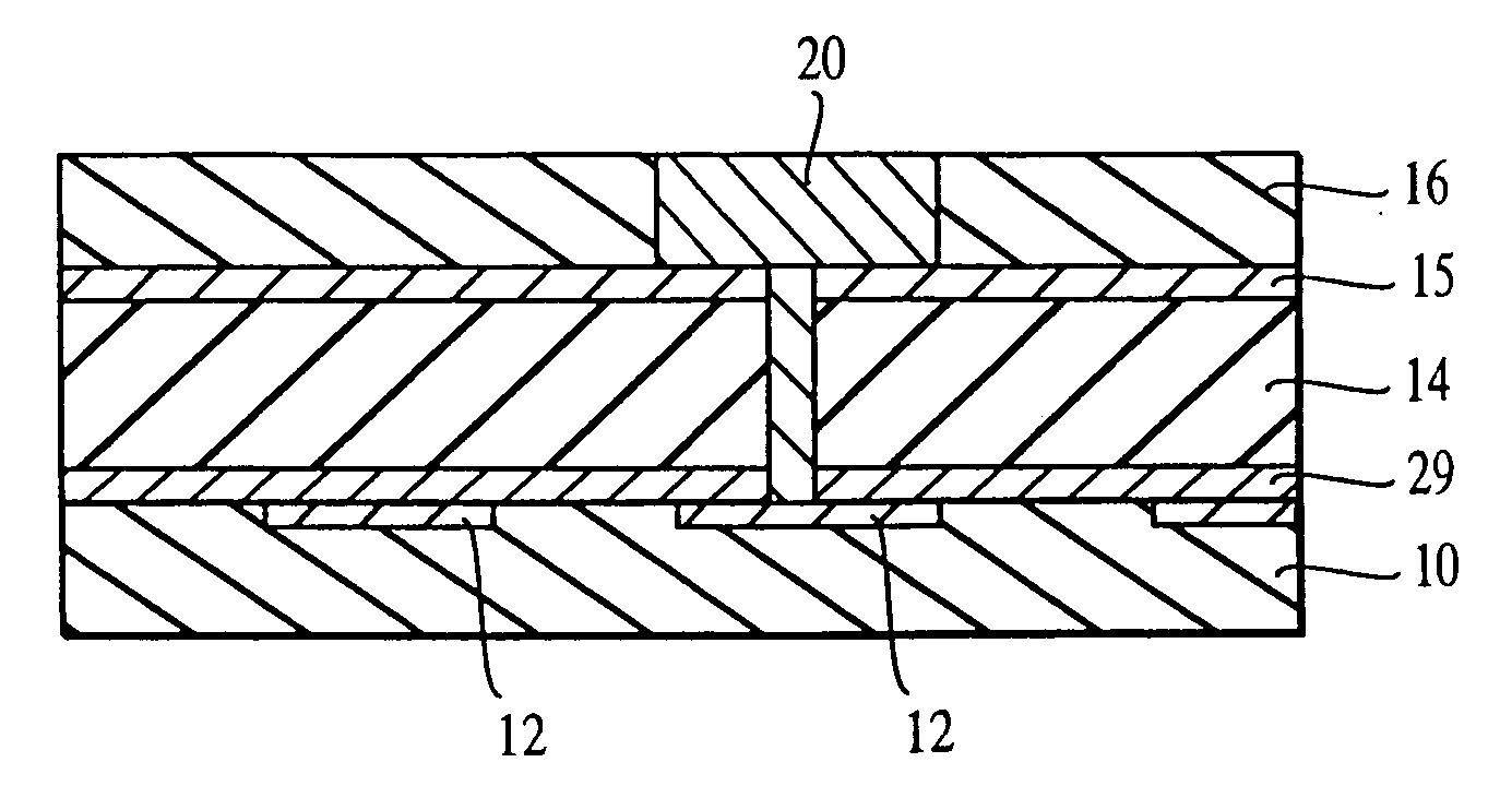
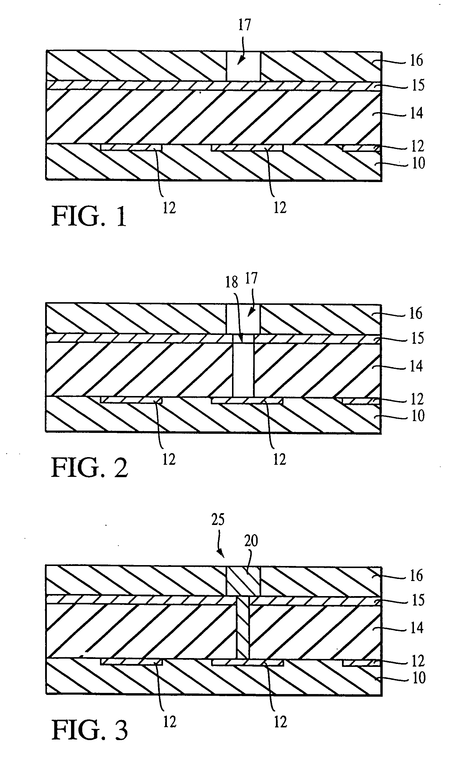
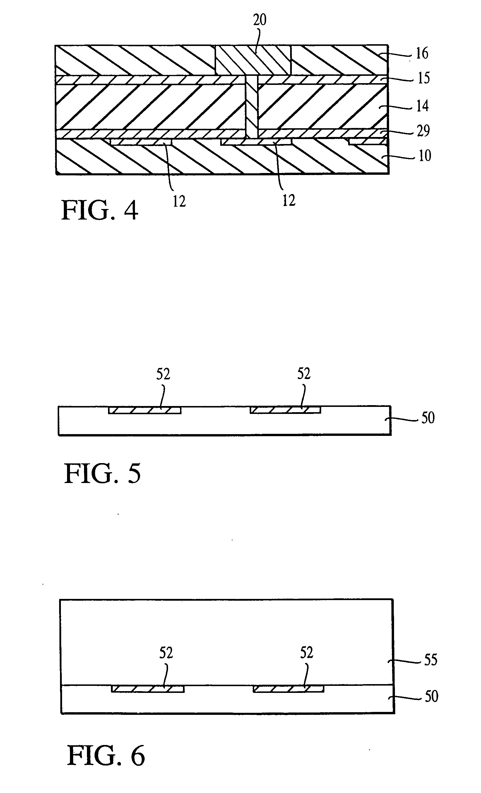
[0010] In an exemplary embodiment, a plurality of low dielectric constant materials are selected with similar methods of formation, as well as with similar capacities to withstand physical and thermal stress. The low dielectric constant materials act as insulating layers through which trenches and vias are subsequently formed by employing a timed etching. Since the low dielectric constant materials are selected so that the etchant available for each one has only a small etch rate relative to the other low dielectric constant materials, the plurality of low dielectric constant materials act as etch stops during the fabrication of damascene structures. This way, the etch stop layers employed in the prior art are eliminated and the number of fabrication steps is reduced.

Problems solved by technology

The integration of a large number of components on a single integrated circuit (IC) chip requires complex interconnects.
Damascene processes such as the ones described above pose significant problems.
One of the problems is caused by the use of one or more etch stop layers.
Although the advantages of using the etch stop layers are significant, the process is complex since separate depositions are required for the etch stop layers.
In addition, the most commonly used etch stop material, silicon nitride (Si3N4), has a rather high dielectric constant (k) (approximately 7), which does not satisfy anymore the requirement of resistance-capacitance delay regarding the parasitic capacitance generated by an intermetal insulating layer.
Silicon nitride does not satisfy the requirement of small stray capacitance of advanced damascene structures.

Method used


Image

  • Etch stop in a damascene interconnect structure
  • Etch stop in a damascene interconnect structure
  • Etch stop in a damascene interconnect structure

Examples


Embodiment Construction

[0036] In the following detailed description, reference is made to various specific embodiments in which the invention may be practiced. These embodiments are described with sufficient detail to enable those skilled in the art to practice the invention, and it is to be understood that other embodiments may be employed, and that structural and electrical changes may be made without departing from the spirit or scope of the present invention.

[0037] The term “substrate” used in the following description may include any semiconductor-based structure that has a semiconductor surface. The term should be understood to include silicon, silicon-on insulator (SOI), silicon-on sapphire (SOS), doped and undoped semiconductors, epitaxial layers of silicon supported by a base semiconductor foundation, and other semiconductor structures. The semiconductor need not be silicon-based. The semiconductor could be silicon-germanium, germanium, or gallium arsenide. When reference is made to a “substrate...


PUM

PropertyMeasurementUnit
dielectric constantaaaaaaaaaa
thicknessaaaaaaaaaa
thicknessaaaaaaaaaa

Abstract

An interconnect structure with a plurality of low dielectric constant insulating layers acting as etch stops is disclosed. The low dielectric constant materials act as insulating layers through which trenches and vias are subsequently formed by employing a timed etching. Since the low dielectric constant materials are selected so that the etchant available for each one has only a small etch rate relative to the other low dielectric constant materials, the plurality of low dielectric constant materials act as etch stops during the fabrication of interconnect structures. This way, the etch stop layers employed in the prior art are eliminated and the number of fabrication steps is reduced.

Description

FIELD OF THE INVENTION [0001] The present invention relates to semiconductor devices and methods of making such devices. More particularly, the invention relates to a method of providing an etch stop in damascene interconnect structures. BACKGROUND OF THE INVENTION [0002] The integration of a large number of components on a single integrated circuit (IC) chip requires complex interconnects. Ideally, the interconnect structures should be fabricated with minimal signal delay and optimal packing density. The reliability and performance of integrated circuits may be affected by the qualities of their interconnect structures. [0003] Advanced multiple metallization layers have been used to accommodate higher packing densities as devices shrink below sub-0.25 micron design rules. One such metallization scheme is a dual damascene structure formed by a dual damascene process. The dual damascene process is a two-step sequential mask / etch process to form a two-level structure, such as a via co...

Claims


Application Information

Patent Timeline
Patent Type & Authority Applications(United States)
IPC IPC(8): H01L23/48H01L21/768H01L23/532
CPCH01L21/76811H01L21/76813H01L21/76835H01L23/53295H01L23/53223H01L23/5329H01L23/5226H01L2924/0002H01L2924/00
Inventor FARRAR, PAUL A.
Owner ROUND ROCK RES LLC
Learn More