Method of manufacturing semiconductor substrate and method of manufacturing semiconductor device

a manufacturing method and semiconductor technology, applied in the direction of semiconductor devices, basic electric elements, electrical appliances, etc., can solve the problems of difficult to stabilize the characteristics the thickness of the soi layer is large, and the cost of soi transistors is higher than that of field effect transistors formed, etc., to achieve the effect of reducing the restriction on the area of the semiconductor layer, reducing the cost and improving the etching rate ratio

Inactive Publication Date: 2006-06-01
SEIKO EPSON CORP
View PDF5 Cites 4 Cited by
  • Summary
  • Abstract
  • Description
  • Claims
  • Application Information

AI Technical Summary

Benefits of technology

[0009] An advantage of the present invention is to provide a method of manufacturing a semiconductor substrate and a method of manufacturing a semiconductor device, which make it possible to form a semiconductor layer on an insulator at low cost while alleviating a restriction on the area of the semiconductor layer which-can be formed on the insulator.
[0010] According to an aspect of the present invention, there is provided a method of manufacturing a semiconductor device, the method comprising: forming a γ-aluminum oxide layer on a semiconductor substrate; forming a semiconductor layer on the γ-aluminum oxide layer; forming an exposed portion for exposing a part of the γ-aluminum oxide layer through the semiconductor layer; forming a support which is formed of a material having an etching rate smaller than that of the γ-aluminum oxide layer and which supports the semiconductor layer on the semiconductor substrate; forming a cavity, which the γ-aluminum oxide layer is removed from, between the semiconductor substrate and the semiconductor layer by selectively etching the γ-aluminum oxide layer through the exposed portion; and forming a buried insulating layer in the cavity by thermally oxidizing the semiconductor substrate and the semiconductor layer inside the cavity through the exposed portion.
[0011] Accordingly, it is possible to increase the etching rate ratio between the semiconductor layer and the γ-aluminum oxide layer while making it possible to form the semiconductor layer on the γ-aluminum oxide layer by the use of epitaxial growth. Therefore, since the γ-aluminum oxide layer can be selectively etched while preventing the semiconductor layer from being etched, it is possible to prevent the restriction to the etching area of the γ-aluminum oxide layer under the semiconductor layer. As a result, it is possible to increase the area of the semiconductor layer which can be formed on the insulating layer while suppressing the deterioration in crystal quality of the semiconductor layer. That is, it is possible to form the semiconductor layer with excellent crystal quality on the insulating layer at low cost.
[0012] In addition, since the γ-aluminum oxide layer can be removed with the semiconductor left by forming the semiconductor layer on the γ-aluminum oxide layer, it is possible to form the cavity under the semiconductor layer. Furthermore, by providing the support for supporting the semiconductor layer on the semiconductor substrate, it is possible to prevent the semiconductor layer from collapsing. As a result, since the semiconductor layer can be formed on the insulating layer while reducing the generation of defects in the semiconductor layer, it is possible to electrically isolate the semiconductor layer from the semiconductor substrate without damaging the quality of the semiconductor layer.
[0013] According to another aspect of the invention, there is provided a method of manufacturing a semiconductor device, the method comprising: forming a γ-aluminum oxide layer on a semiconductor substrate; forming a semiconductor layer on the γ-aluminum oxide layer; forming a first groove for exposing the semiconductor substrate through the γ-aluminum oxide layer and the semiconductor layer; forming in the first groove a support which is formed on the sidewalls of the γ-aluminum oxide layer and the semiconductor layer and has an etching rate smaller than that of the γ-aluminum oxide layer; forming a second groove for exposing at least a part of the γ-aluminum oxide layer, in which the support is formed on the sidewalls thereof, through the semiconductor layer; forming a cavity, which the γ-aluminum oxide layer is removed from, between the semiconductor substrate and the γ-aluminum oxide layer by selectively etching the γ-aluminum oxide layer through the second groove; and forming a buried insulating layer in the cavity by thermally oxidizing the semiconductor substrate and the semiconductor layer inside the cavity through the first groove and the second groove.
[0014] Accordingly, it is possible to increase the etching rate ratio between the semiconductor layer and the γ-aluminum oxide layer while making it possible to form the semiconductor layer on the γ-aluminum oxide layer by the use of epitaxial growth. As a result, it is possible to increase the area of the semiconductor layer which can be formed on the insulating layer while suppressing the deterioration in crystal quality of the semiconductor layer.

Problems solved by technology

As a result, the SOI transistor requires a cost higher than that of field effect transistors formed in a bulk semiconductor substrate.
In addition, there are problems in that the deviation in thickness of the SOI layer is great in the ion-implanting or the polishing and that when the SOI layer is thinned to manufacture a complete depletion-mode SOI transistor, it is difficult to stabilize the characteristics of the field effect transistors.
's paper, since only the SiGe layer is selectively removed by the use of a selectivity ratio between Si and SiGe, there is a problem in that the etching distance of the SiGe layer is restricted and the area of the SOI layer is restricted.
However, when the concentration of Ge in the SiGe layer increases, it is difficult to increase the thickness of the SiGe layer while maintaining the crystal quality.
Accordingly, the thickness of the BOX layer decreases and the crystal quality of the Si layer formed on the SiGe layer deteriorates, thereby reducing the characteristics of the SOI transistor.

Method used


Image

  • Method of manufacturing semiconductor substrate and method of manufacturing semiconductor device
  • Method of manufacturing semiconductor substrate and method of manufacturing semiconductor device
  • Method of manufacturing semiconductor substrate and method of manufacturing semiconductor device

Examples


Embodiment Construction

[0037] A method of manufacturing a semiconductor device according to exemplary embodiments of the present invention will be described with reference to the drawings.

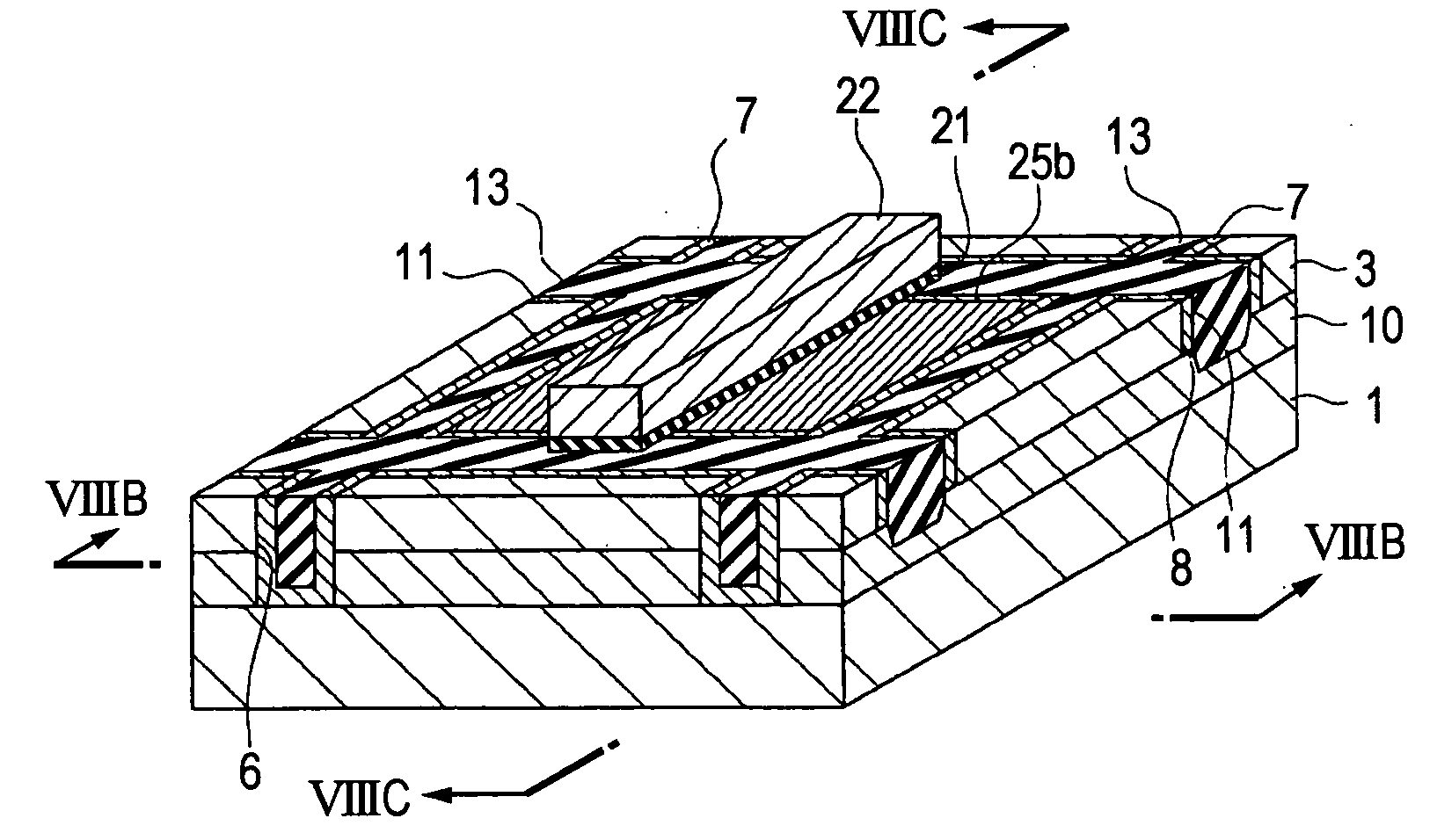
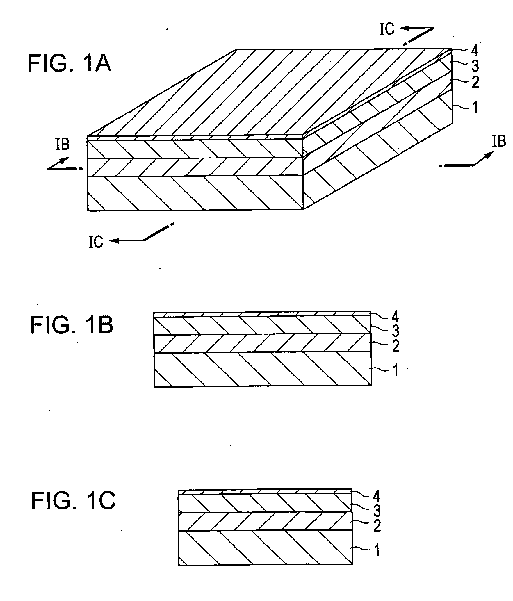
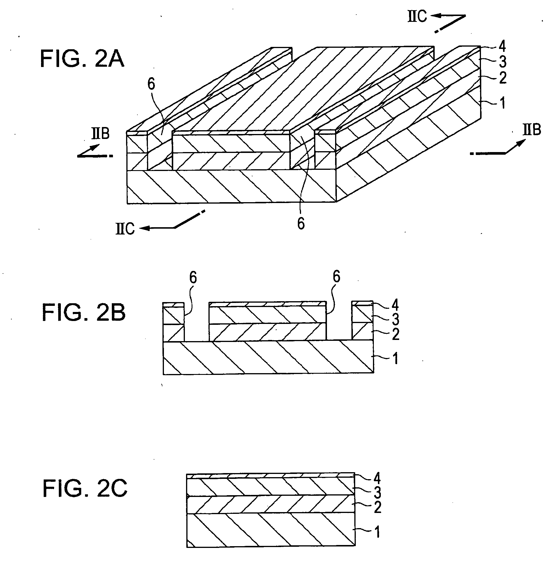
[0038]FIGS. 1A to 8A are perspective views illustrating a method of manufacturing a semiconductor device according to an embodiment of the invention, FIGS. 1B to 8B are cross-sectional views taken along Lines A1-A1′ to A8-AB′ of FIGS. 1A to 8A, respectively, and FIGS. 1C to 8C are cross-sectional views taken along Lines B1-B1′ to B8-B8′ of FIGS. 1A to 8A, respectively.

[0039] Referring to FIG. 1, a γ-aluminum oxide layer ( γ-Al2O3 layer) 2 is formed on a semiconductor substrate 1 by the use of epitaxial growth and a semiconductor layer 3 is formed on the γ-aluminum oxide layer 2 by the use of epitaxial growth. The semiconductor substrate 1 and the semiconductor layer 3 may be formed of, for example, Si, Ge, SiGe, SiC, SiSn, PbS, GaAs, InP, GaP, GaN, ZnSe, or the like. Specifically, when the semiconductor substrate 1 is ...


PUM

PropertyMeasurementUnit
capacitanceaaaaaaaaaa
speedaaaaaaaaaa
concentrationaaaaaaaaaa

Abstract

There is provided a method of manufacturing a semiconductor device, the method including: forming a γ-aluminum oxide layer on a semiconductor substrate; forming a semiconductor layer on the γ-aluminum oxide layer; forming an exposed portion for exposing a part of the γ-aluminum oxide layer through the semiconductor layer; forming a support which is formed of a material having an etching rate smaller than that of the γ-aluminum oxide layer and which supports the semiconductor layer on the semiconductor substrate; forming a cavity, which the γ-aluminum oxide layer is removed from, between the semiconductor substrate and the semiconductor layer by selectively etching the γ-aluminum oxide layer through the exposed portion; forming a buried insulating layer in the cavity by thermally oxidizing the semiconductor substrate and the semiconductor layer inside the cavity through the exposed portion; forming a gate electrode on the semiconductor layer with a gate insulating layer therebetween; and forming source/drain layers, which are disposed on both sides of the gate electrode, in the semiconductor layer.

Description

BACKGROUND [0001] 1. Technical Field [0002] The present invention relates to a method of manufacturing a semiconductor substrate and a method of manufacturing a semiconductor device and more particularly to a method of manufacturing a semiconductor device, which can be suitably used for a field effect transistor formed on an SOI (Silicon On Insulator) substrate. [0003] 2. Related Art [0004] The usefulness of field effect transistors formed on an SOI (Silicon On Insulator) substrate has attracted much attention, in that isolation of semiconductor devices is easy, latch-up does not occur, and source-drain junction capacitance is small. Particularly, since full depletion-mode SOI transistors have low power consumption, can operate at a high speed, and can be easily driven with low voltage, studies for allowing the SOI transistors to operate in the complete depletion mode have vigorously advanced. Here, for example, as disclosed in Japanese Unexamined Patent Application Publication Nos....

Claims


Application Information

Patent Timeline
Patent Type & Authority Applications(United States)
IPC IPC(8): H01L21/84
CPCH01L21/76283H01L29/66772H01L29/78603H01L29/78654
Inventor HARA, TOSHIKI
Owner SEIKO EPSON CORP
Why Eureka
Try Eureka