Unlock instant, AI-driven research and patent intelligence for your innovation.

Array substrate and method of manufacturing the same, and display device

Active Publication Date: 2018-06-21
BOE TECH GRP CO LTD +1
View PDF3 Cites 1 Cited by
  • Summary
  • Abstract
  • Description
  • Claims
  • Application Information

AI Technical Summary

Benefits of technology

The present invention provides a method to reduce panel stain caused by poor diffusion of PI solution or metal solution on edges of common holes or connection holes in an array substrate. By improving coating of PI solution or metal solution and reducing section drop of common holes or connection holes, the method helps to prevent staining of the panel and improve the quality of the finished product.

Problems solved by technology

Subsequently, during the subsequent assembling of cells, when the PI solution is used to form a guide film, problems such as poor diffusion (for example, non-uniform) of PI solution at edges of the common holes in the common electrode will occur, and thus panel stain will appear.
A top-gate structure array substrate also involves the same problems.
When forming connection holes in the gate insulating layer to electrically connect with the source / drain electrodes of thin film transistors and a pixel electrode pattern / data line pattern, the problems such as poor diffusion (for example, non-uniform) of the PI solution at edges of the connection holes in the common electrode will also occur and thus panel stain will appear.

Method used


Image

  • Array substrate and method of manufacturing the same, and display device
  • Array substrate and method of manufacturing the same, and display device
  • Array substrate and method of manufacturing the same, and display device

Examples


Embodiment Construction

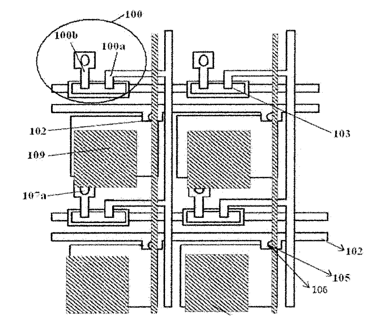
[0023]Other features and advantages of various embodiments and structures and operations thereof will be described in detail with reference to the drawings. It is noted that the present invention is not limited to the embodiments in the specification. These embodiments are illustrated in the specification for illustration only. Based on the teaching included herein, it is obvious for those skilled in the art to obtain additional embodiments.

[0024]It is noted that “an / one embodiment”, “embodiments” and “exemplary embodiment(s)” referred in the specification mean that the described embodiment may include specific feature, structure or characteristic, and however, it is not necessary that every embodiment includes the specific feature, structure or characteristic. Furthermore, the above wordings do not necessarily denote the same embodiment. In addition, it is understood that, when the specific feature, structure or characteristic are described in conjunction with embodiments, implemen...


PUM


Abstract

There is disclosed a method of manufacturing an array substrate, the method including a step of forming thin film transistors on a substrate; wherein the step of forming the thin film transistors on the substrate includes: forming a first electrically conductive layer on the substrate; forming an insulating layer on the first electrically conductive layer; forming at least one common holes in the insulating layer to communicate with the first electrically conductive layer; forming a first connection portion, which is made of the same material as a second electrically conductive layer, in the at least one of the at least one common holes while forming the second electrically conductive layer on the insulating layer by using a single process, the first connection portion being in electrical contact with the first electrically conductive layer. In addition, there is disclosed an array substrate manufactured by the above method and a display device including the array substrate.

Description

CROSS-REFERENCE TO RELATED APPLICATIONS[0001]The present application is a Section 371 National Stage application of International Application No. PCT / CN2016 / 082791, filed 20 May 2016, which has not yet published, and claims priority to Chinese Patent Application No. 201610200608.8, filed on Mar. 31, 2016, entitled “array substrate and method of manufacturing the same, and display device”, which are incorporated herein by reference in their entirety.BACKGROUND1. Technical Field[0002]The present disclosure relates to technical field of liquid crystal display, and particularly to an array substrate and a method of manufacturing the same and a display device including the array substrate.2. Description of the Related Art[0003]In liquid crystal display technology, common electrodes may be configured at a side of a color film substrate or at a side of an array substrate. In the case where the common electrodes are configured at a side of the array substrate (bottom-gate structure), a sect...

Claims


Application Information

Patent Timeline
IPC IPC(8): G02F1/1362G02F1/1343G02F1/1368
CPCG02F1/136286G02F1/13439G02F1/1368G02F1/134363G02F2001/136295G02F2001/13685G02F2201/121G02F1/134336G02F1/136227H01L27/124H01L27/1259G02F1/1362G02F1/134372G02F1/13685G02F1/136295H01L27/12
Inventor SONG, BOTAOLIN, LIANGMA, TAOWANG, WENLONGHAN, LINGWEI, YU
Owner BOE TECH GRP CO LTD