Wiring substrate, method for manufacturing wiring substrate, and semiconductor package including wiring substrate

Active Publication Date: 2011-07-14
SHINKO ELECTRIC IND CO LTD
View PDF6 Cites 18 Cited by
  • Summary
  • Abstract
  • Description
  • Claims
  • Application Information

AI Technical Summary

Benefits of technology

[0017]The present invention may provide a wiring substrate, a method for manufacturing the wiring substrate, and a semiconductor package includi

Problems solved by technology

However, it is becoming difficult to satisfy such desire with the wiring sub

Method used


Image

  • Wiring substrate, method for manufacturing wiring substrate, and semiconductor package including wiring substrate
  • Wiring substrate, method for manufacturing wiring substrate, and semiconductor package including wiring substrate
  • Wiring substrate, method for manufacturing wiring substrate, and semiconductor package including wiring substrate

Examples


first embodiment

(Configuration of Wiring Substrate)

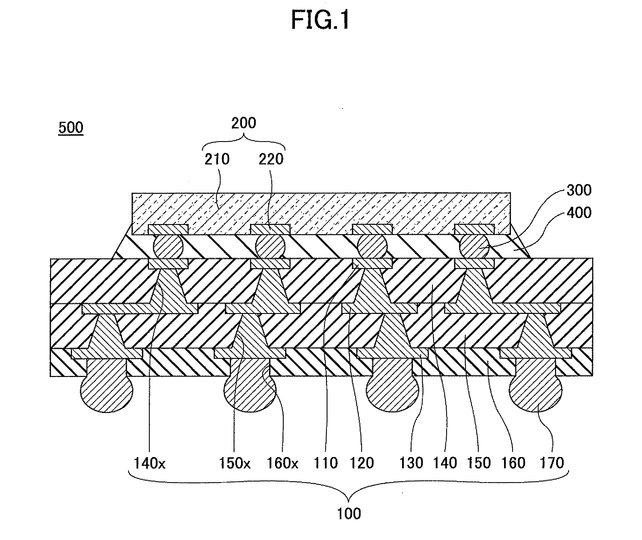
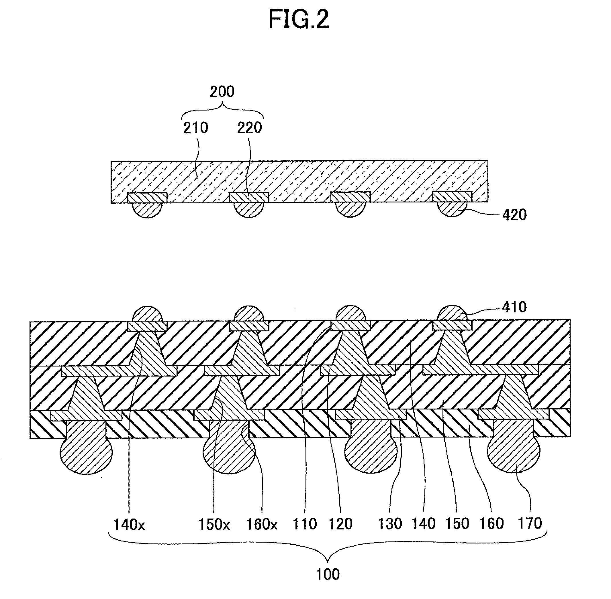
[0051]An exemplary configuration of a wiring substrate 10 including a ceramic substrate 20 and a silicon substrate 30 is described. FIG. 4 is a cross-sectional view illustrating an example of the wiring substrate 10 according to the first embodiment of the present invention. With reference to FIG. 4, the wiring substrate 10 has the silicon substrate 30 bonded onto a ceramic substrate 20 via a polymer layer 40 (i.e. so-called polymer bonded structure). An outer connection terminal(s) 29 is provided in the ceramic substrate 20.

[0052]In this embodiment, the wiring substrate 10 has a rectangular shape. The wiring substrate 10 may be formed having a width of, for example, approximately 15 mm (X direction) and a depth of, for example, approximately 15 mm (Y direction). The ceramic substrate 20 may be formed having a thickness of, for example, approximately 50-1000 μm (Z direction). The silicon substrate 30 may be formed having a thickness of, for example...

second embodiment

[0125]Next, a method for manufacturing the wiring substrate 10 illustrated in FIG. 4 according to a second embodiment of the present invention is described. FIGS. 19-23B are schematic diagrams illustrating steps of manufacturing the wiring substrate 10 according to the second embodiment of the present invention. In FIGS. 9-23B, like components are denoted with like reference numerals as of those of FIG. 4 and are not further explained.

[0126]First, in the step illustrated in FIG. 19, a substrate body 31T is prepared by performing the steps illustrated in FIGS. 5-8 of the first embodiment of the present invention. The substrate body 31T has an insulating layer 32 formed on the first surface 31a of the substrate body 31T and an inner side surface of the via holes 31y. The substrate body 31T may be formed having a thickness of, for example, approximately 50-500 μm. Further, plural independent ceramic substrates 20, which are obtained by dividing the ceramic substrate 20S, are prepared. ...

third embodiment

[0138]Next, an example of a semiconductor package 80 having a semiconductor chip 81 mounted on the wiring substrate 10 of FIG. 4 according to a third embodiment of the present invention is described. In the third embodiment, like components are denoted with like reference numerals as of those of the first embodiment and are not further explained.

(Configuration of Semiconductor Package)

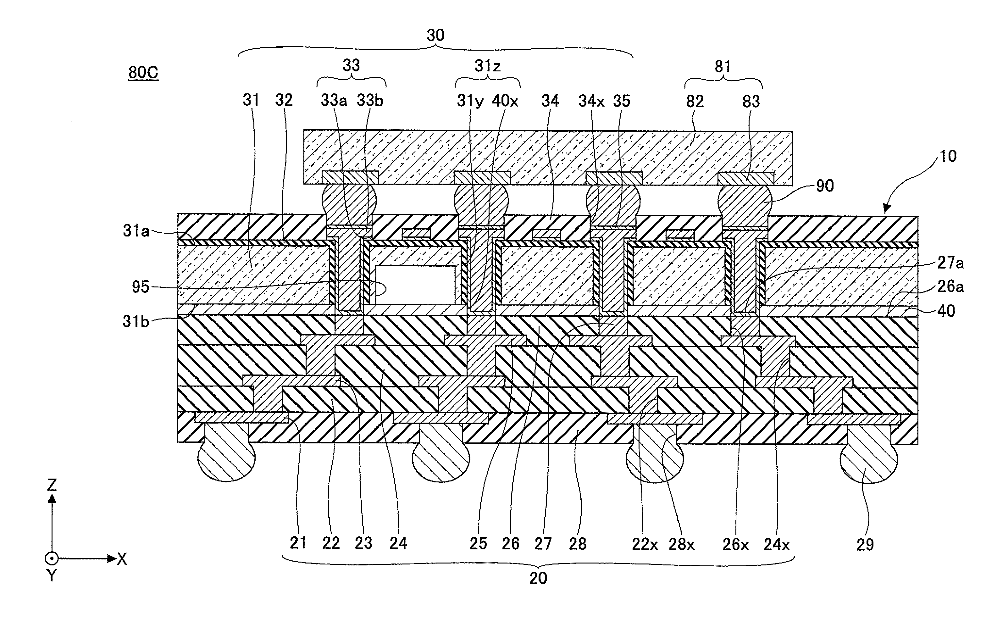
[0139]Next, an exemplary configuration of the semiconductor package 80 according to the third embodiment of the present invention is described. FIG. 24 is a cross-sectional view of an example of the semiconductor package 80 according to the third embodiment of the present invention. In FIG. 24, like components are denoted with like reference numerals as of those of the FIG. 4 and are not further explained. In the example illustrated in FIG. 24, the semiconductor package 80 includes the wiring substrate 10 of FIG. 4, the semiconductor chip 81, and plural solder bumps 90.

[0140]The semiconductor chip 81 i...


PUM


Abstract

A wiring substrate includes a ceramic substrate including plural ceramic layers, an inner wiring, and an electrode electrically connected to the inner wiring, the electrode exposed on a first surface of the ceramic substrate, and a silicon substrate body having a front surface and a back surface situated on an opposite side of the front surface and including a wiring pattern formed on the front surface and a via filling material having one end electrically connected to the wiring pattern and another end exposed at the back surface. The back surface is bonded to the first surface of the ceramic substrate via a polymer layer. The via filling material penetrates through the polymer layer and is directly bonded to the electrode.

Description

CROSS-REFERENCE TO RELATED APPLICATIONS[0001]This application is based upon and claims the benefit of priority of the prior Japanese Priority Application No. 2010-004394 filed on Jan. 12, 2010, the entire contents of which are incorporated herein by reference.BACKGROUND OF THE INVENTION[0002]1. Field of the Invention[0003]The present invention generally relates to a wiring substrate, a method for manufacturing the wiring substrate, and a semiconductor package including the wiring substrate.[0004]2. Description of the Related Art[0005]There is known a semiconductor package having a semiconductor chip mounted on a wiring substrate via solder bumps or the like. In this semiconductor package, the wiring substrate acts as an interposer during a process of connecting the semiconductor chip to a target substrate (e.g., motherboard). A related art example of a semiconductor package 500 having a wiring substrate 100 acting as an interposer is described with reference to FIG. 1.[0006]FIG. 1 i...

Claims


Application Information

Patent Timeline
IPC IPC(8): H01L29/92H01L23/538H01L21/762
CPCH01L21/4857H01L23/147H01L2924/1461H01L2924/10253H01L2924/15311H01L23/49822H01L23/49827H01L23/49894H01L28/40H01L2924/09701H01L2224/16225H01L2924/00H01L2224/32225H01L2224/73204H01L2924/15174
Inventor ARAI, TADASHI
Owner SHINKO ELECTRIC IND CO LTD
Why Eureka
Try Eureka