Capacitive fingerprint sensing device comprising display functionality

Active Publication Date: 2018-06-21
FINGERPRINT CARDS ANACATUM IP AB
View PDF0 Cites 10 Cited by
  • Summary
  • Abstract
  • Description
  • Claims
  • Application Information

AI Technical Summary

Benefits of technology

The patent text is about a fingerprint sensing element that uses a capacitive coupling between a finger and electrodes on a protective layer. The protective layer is made of a hard and durable material like glass or ceramic. The adapting of a bias over a diode in the element can be achieved by controlling the potential on the electrodes. This helps to minimize current and ensure good capacitive coupling. The technical effect of this invention is to provide a reliable and accurate fingerprint sensing device.

Problems solved by technology

However, the TFT-technology is limiting in that a display typically comprises 1-6 transistors per pixel, whereas a fingerprint sensor typically requires significantly more transistors, which is difficult to achieve for a TFT display.
Accordingly, circuitry for high resolution capacitive fingerprint sensing can not easily be implemented in TFT technology.
However, the biasing must be controlled such that the current flowing through the diode in the fingerprint sensing mode is not so large so that it significantly degrades the fingerprint sensing functionality.

Method used


Image

  • Capacitive fingerprint sensing device comprising display functionality
  • Capacitive fingerprint sensing device comprising display functionality
  • Capacitive fingerprint sensing device comprising display functionality

Examples


Embodiment Construction

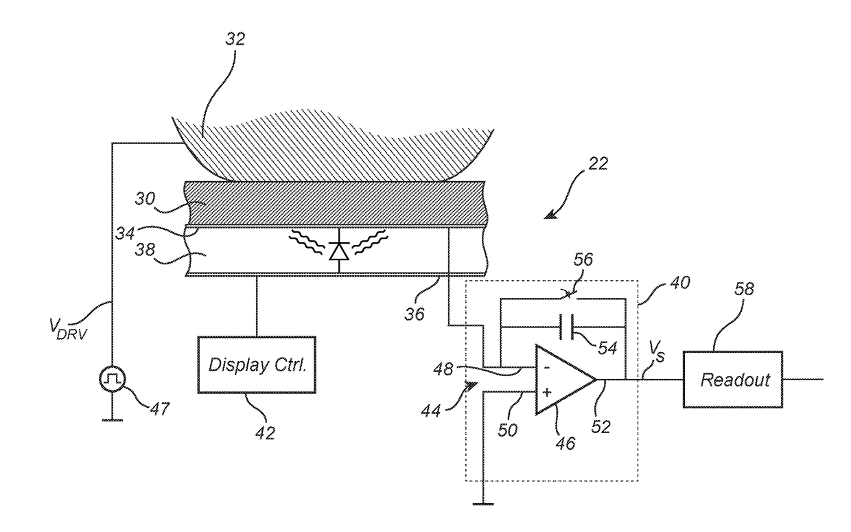
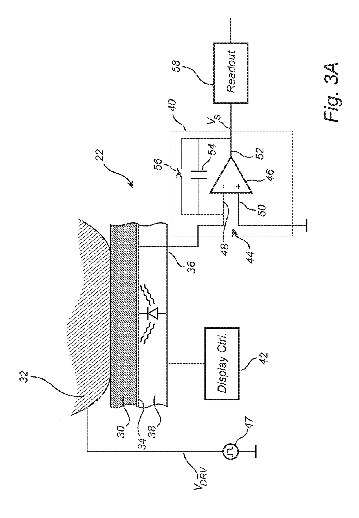
[0046]In the present detailed description, various embodiments of the system and method according to the present invention are mainly described with reference to a capacitive fingerprint sensing device arranged in a smartphone. However, it should be noted that the present invention is applicable in a wide range of applications.

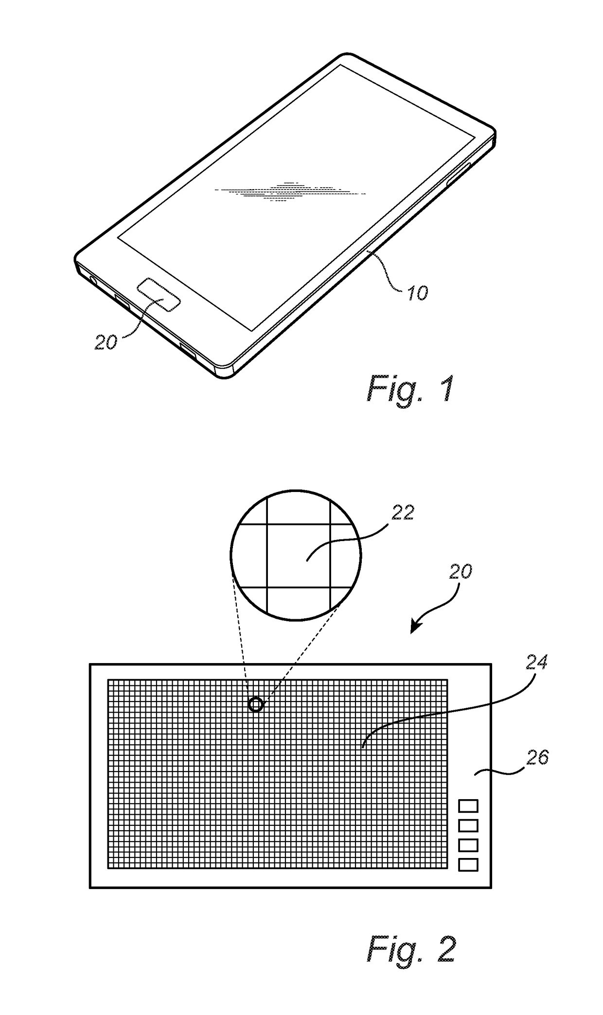
[0047]FIG. 1 schematically illustrates a smartphone 10 comprising a fingerprint sensing device 20 according to an example embodiment of the present invention. The fingerprint sensing device 20 may, for example, be used for unlocking the smartphone 10 and / or for authorizing transactions carried out using the smartphone, etc. A fingerprint sensing device according to various embodiments of the invention may also be used in other devices, such as tablet computers, laptops, smartcards or other types of consumer electronics. The described fingerprint sensing device may also be used in applications such as smartcards, vehicles etc.

[0048]FIG. 2 schematically shows th...


PUM


Abstract

A capacitive fingerprint sensing device for sensing a fingerprint pattern of a finger can comprise a plurality of sensing elements. Each sensing element comprises a protective dielectric top layer to be touched by the finger; a first electrode comprising an optically transparent electrically conductive sensing structure arranged underneath the top layer; fingerprint sensing circuitry connected to the first electrode and configured to provide an analog sensing signal indicative of a distance between the finger and the sensing structure, a second electrode arranged underneath the first electrode; an organic light emitting layer arranged between the first and second electrodes; display element control circuitry connected to the second electrode and configured to control a display element comprising the first and second electrodes and the organic light emitting layer; and a switching mechanism configured to switch the sensing element between a fingerprint sensing mode and a display mode.

Description

CROSS REFERENCE TO RELATED APPLICATIONS[0001]This application claims priority to Sweden Application No. 1651678-3 filed on Dec. 19, 2016, the disclosure of which is incorporated herein by reference in its entirety.FIELD OF THE INVENTION[0002]The present invention relates to a capacitive fingerprint sensing device comprising a display element integrated in the capacitive sensing elementBACKGROUND OF THE INVENTION[0003]The integration of a fingerprint sensor in a display panel is very desirable for the mobile fingerprint sensing industry. A conventional approach to address this challenge has been to integrate a fingerprint sensor in a common display panel such as an LCD panel or an OLED panel. In this approach, the priority is given to display properties and visual quality. Therefore, the final desired product is a display panel which is capable of detecting a fingerprint.[0004]In a display having fingerprint sensing capabilities, the pixels in the display are also acting as capacitiv...

Claims


Application Information

Patent Timeline
IPC IPC(8): G06K9/00G06F3/041G06F3/044H01L27/32G06V30/144G06V40/13H10K59/40
CPCG06K9/0002G06F3/0416G06F3/044H01L27/323G06F2203/04112G06F3/0412G06F3/0445G06V40/1306H10K59/40
Inventor GHAVANINI, FARZANJAGEMALM, PONTUS
Owner FINGERPRINT CARDS ANACATUM IP AB
Why Eureka
Try Eureka