

Delay circuit, count value generation circuit, and physical quantity sensor
a technology of count value generation and delay circuit, applied in the direction of logic circuits characterised by logic functions, counting chain synchronous pulse counters, pulse techniques, etc., can solve the problems of circuit scale increase and power consumption increase, and achieve high precision
- Summary
- Abstract
- Description
- Claims
- Application Information
AI Technical Summary
Benefits of technology
Problems solved by technology
Method used
Image

Examples
first embodiment
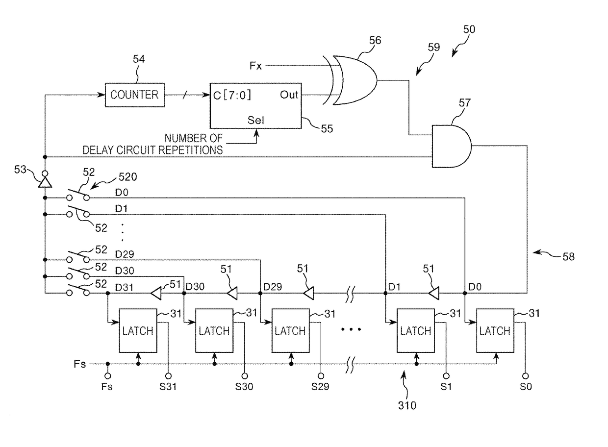
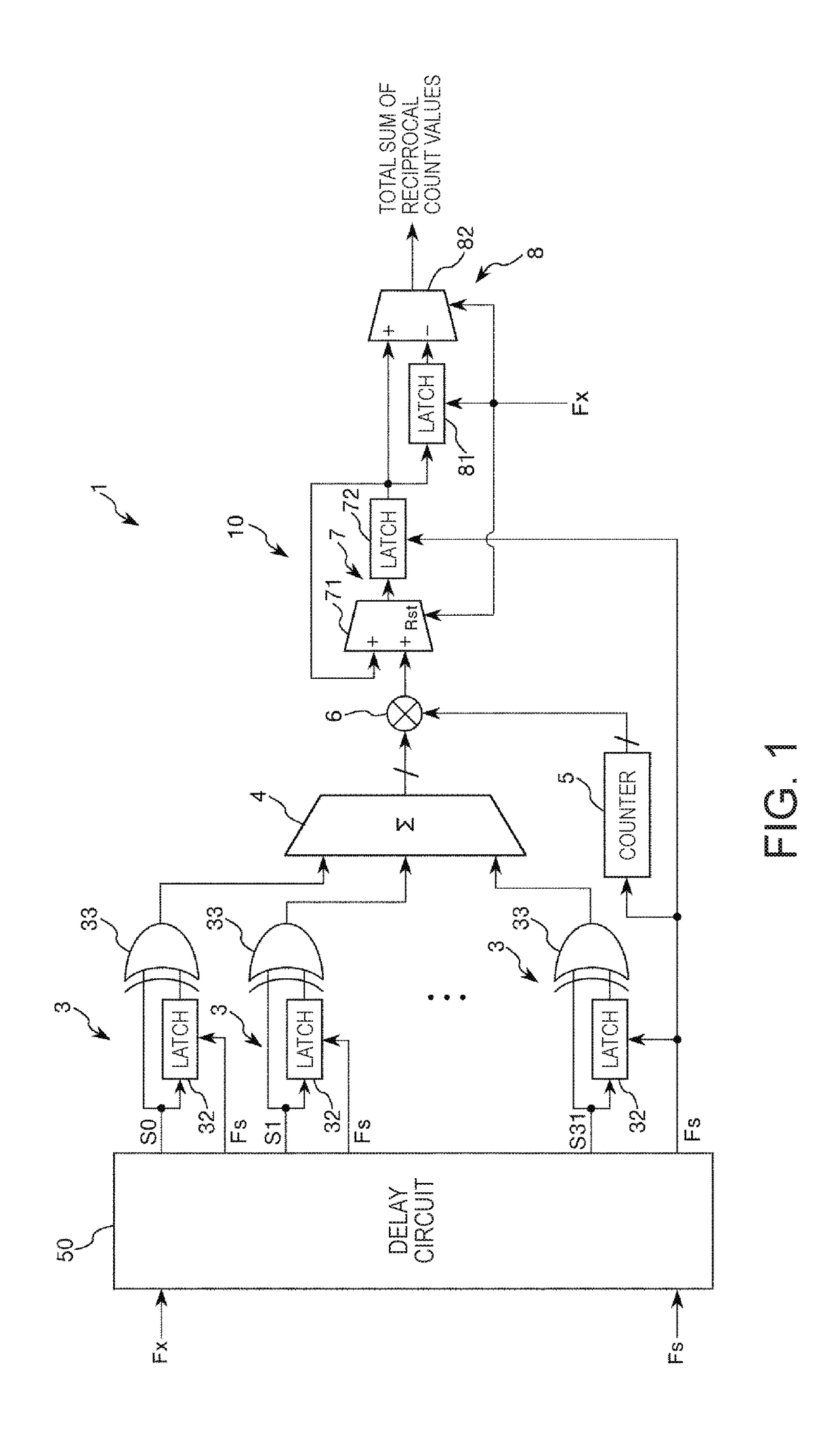
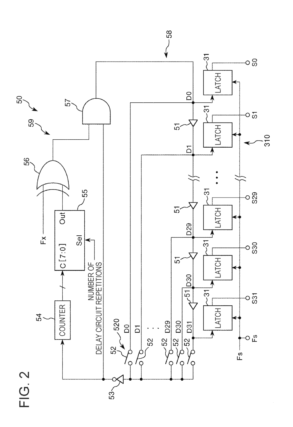
[0041]FIG. 1 is a block diagram illustrating a first embodiment of a reciprocal count value generation circuit which is one example of a count value generation circuit according to the invention. FIG. 2 is a block diagram illustrating a delay circuit of the reciprocal count value generation circuit illustrated in FIG. 1.
[0042]In the drawing, a measurement signal is denoted by “Fx”, a measurement signal (a measurement signal immediately before input to a latch 31) output from an AND circuit 57 is denoted by “D”, and a signal output from the latch 31 is denoted by “S”. A reference clock (reference signal) is denoted by “Fs”. A plurality of D and a plurality of S are distinguished from each other by appending suffixes (the same applies to the drawing of other embodiments).
[0043]In the following description, signals formed by causing phases of the measurement signals to be different are also referred to as “measurement signals”. A case in which a level of a signal is “low” is referred t...
second embodiment
[0128]FIG. 3 is a block diagram illustrating a second embodiment of the reciprocal count value generation circuit which is one example of the count value generation circuit according to the invention. FIG. 4 is a block diagram illustrating a delay circuit of the reciprocal count value generation circuit illustrated in FIG. 3. FIG. 5 is a timing chart illustrating an operation of the reciprocal count value generation circuit illustrated in FIG. 3. In FIG. 3, a bus in a circuit is indicated by a thick line (the same applies to other drawings).
[0129]In the drawings, to distinguish measurement signals with different phases from each other, suffixes (0, 1, . . . , and 31) are appended to “Fx” (the same applies to the drawings of other embodiments). A reference clock is denoted by “Fs” and a pulse signal that has a pulse synchronized with a rising edge of the reference clock and a pulse synchronized with a falling edge of the reference clock is denoted by “P” (the same applies to the draw...
third embodiment
[0165]FIG. 6 is a block diagram illustrating a third embodiment of the reciprocal count value generation circuit 1 which is one example of the count value generation circuit according to the invention.
[0166]Hereinafter, the third embodiment will be described focusing on differences from the above-described embodiment. The description of the same matters will be omitted.
[0167]In the third embodiment, for the reference clock and the measurement signal, inversion of a signal occurs in both rising and falling of the signal.
[0168]As illustrated in FIG. 6, a reciprocal count value generation circuit 1 according to the third embodiment includes an edge detection unit 9, a delay circuit 50, a counter 11 which is one example of a second counter, a latch 18, counters 30 (only one counter is illustrated in the drawing) which are one example of a plurality of first counters, a plurality of latches (only one latch is illustrated in the drawing), an enumeration unit 19, a multiplier 25, a counter...
PUM
 Abstract
Description
Claims
Application Information