Flash memory structure and method of manufacturing the same

a flash memory and memory technology, applied in the field of memory structure, can solve the problems of poor operation durability, large writing/erase voltage, slow operation speed of the conventional flash memory structure, etc., and achieve the effects of reducing the writing and erase voltage of the memory, increasing the operating speed of elements, and reducing the writing and erase voltag

Active Publication Date: 2018-06-28
NATIONAL TAIWAN NORMAL UNIVERSITY
View PDF4 Cites 9 Cited by
  • Summary
  • Abstract
  • Description
  • Claims
  • Application Information

AI Technical Summary

Benefits of technology

[0006]An objective of the present invention is to provide a flash memory structure and a method of manufacturing the same, to make the flash memory structure of the present invention have characteristics of reduced writing and erase voltages of the memory and increased operating speed of elements.
[0007]The flash memory structure of one embodiment includes a substrate, a source, a drain, a tunnel isolation layer, a ferroelectric-charge-trapping layer, at least one blocking isolation layer and at least one gate. The substrate is made of a semiconductive material. The source is formed on the substrate. The drain is formed on the substrate and spaced apart from the source. The tunnel isolation layer is formed on the substrate. The ferroelectric-charge-trapping layer is formed on the tunnel isolation layer and contains a charge-trapping layer and a ferroelectric negative-capacitance effect layer. The at least one blocking isolation layer is formed on the ferroelectric-charge-trapping layer. The at least one gate is formed on the blocking isolation layer. The ferroelectric negative-capacitance effect layer is made of a material with the ferroelectric negative-capacitance effect.
[0008]A method of making a flash memory structure of one embodiment includes the following steps: providing a substrate made of a semiconductive material; forming a source on the substrate; forming a drain spaced apart from the source on the substrate; forming a tunnel isolation layer on the substrate; forming a ferroelectric-charge-trapping layer on the tunnel isolation layer, the ferroelectric-charge-trapping layer including a charge-trapping layer and a ferroelectric negative-capacitance effect layer; forming at least one blocking isolation layer on the ferroelectric-charge-trapping layer; and forming at least one gate on the blocking isolation layer. The ferroelectric negative-capacitance effect layer is made of a material with the ferroelectric negative-capacitance effect.
[0009]The present invention uses a ferroelectric negative-capacitance effect layer to enable the flash memory structure of the present invention to reduce the writing and erase voltages of the memory and increase the operating speed of elements.

Problems solved by technology

The conventional flash memory structure 1 has a slow operating speed (about 100 μs to 1 ms), a large writing / erase voltage (e.g., greater than 15 V) and poor operation durability (about 105 cycles).
However, the basic transistor physical phenomenon of the conventional flash memory structure 1 makes the minimum value of the S.S. be 60 mV / dec, and the operating voltage and switch power consumption cannot further be reduced.

Method used


Image

  • Flash memory structure and method of manufacturing the same
  • Flash memory structure and method of manufacturing the same
  • Flash memory structure and method of manufacturing the same

Examples


Embodiment Construction

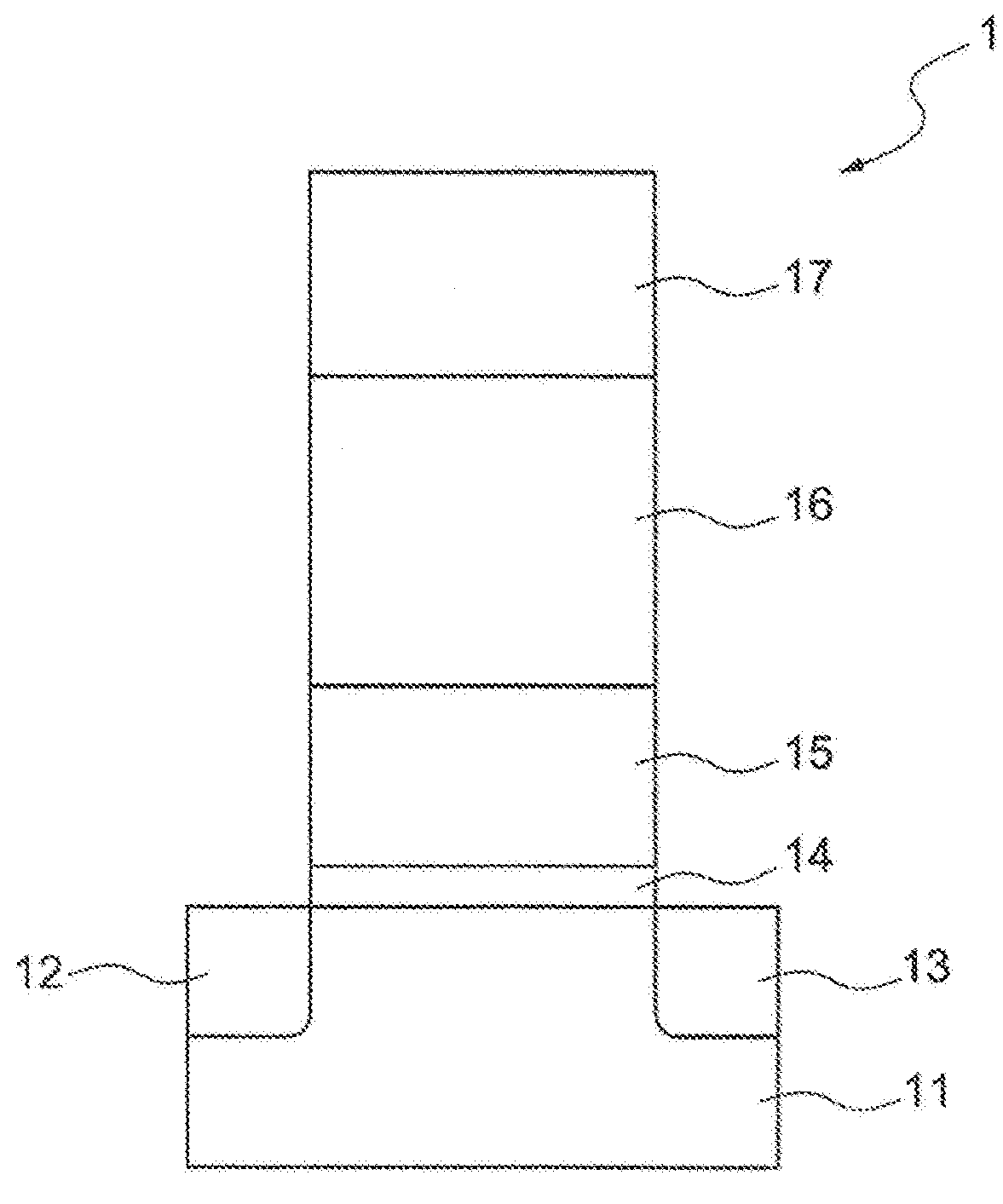
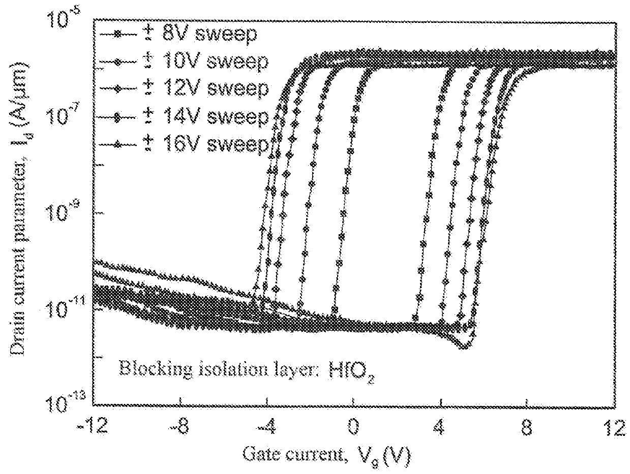
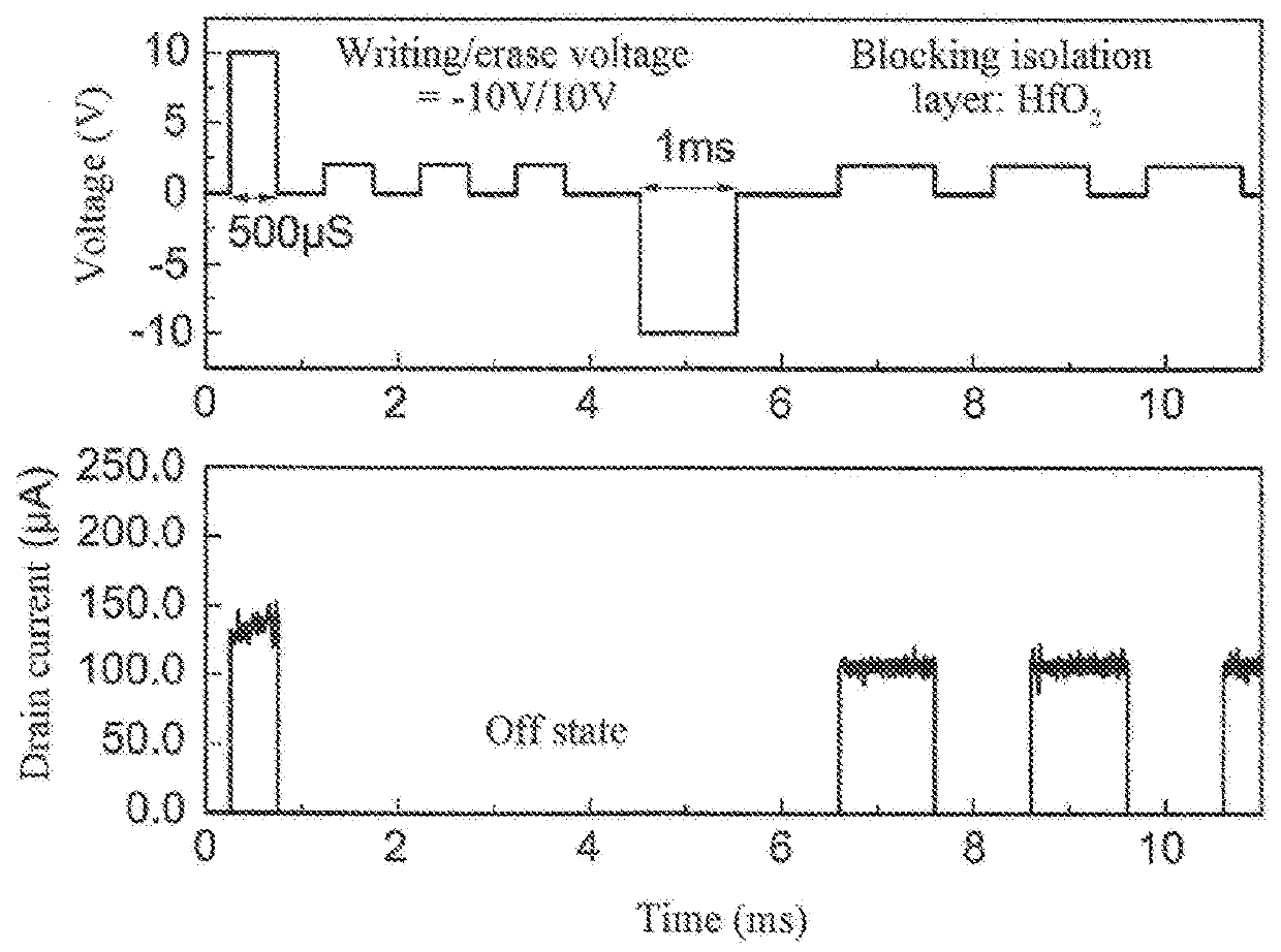
[0019]Referring to FIG. 4, the flash memory structure 3 of one embodiment includes a substrate 31, a source 32, a drain 33, a tunnel isolation layer 34, a ferroelectric-charge-trapping layer 35, at least one blocking isolation layer 36 and at least one gate 37. The substrate 31 is made of a semiconductive material. The source 32 is formed on the substrate 31. The drain 33 is formed on the substrate 31 and spaced apart from the source 32. The tunnel isolation layer 34 is formed on the substrate 31. The ferroelectric-charge-trapping layer 35 is formed on the tunnel isolation layer 34 and contains a charge-trapping layer 351 and a ferroelectric negative-capacitance effect layer 352. The at least one blocking isolation layer 36 is formed on the ferroelectric-charge-trapping layer 35. The at least one gate 37 is formed on the blocking isolation layer 36. The ferroelectric negative-capacitance effect layer 352 is made of a material with the ferroelectric negative-capacitance effect. To im...


PUM


Abstract

A flash memory structure and a method of making the same are provided. The flash memory structure comprises a substrate, a source, a drain, a tunnel isolation layer, a ferroelectric-charge-trapping layer, at least one blocking isolation layer and at least one gate. The substrate is made of a semiconductive material. The source is formed on the substrate. The drain is formed on the substrate and spaced apart from the source. The tunnel isolation layer is formed on the substrate. The ferroelectric-charge-trapping layer is formed on the tunnel isolation layer and contains a charge-trapping layer and a ferroelectric negative-capacitance effect layer. The at least one blocking isolation layer is formed on the ferroelectric-charge-trapping layer. The at least one gate is formed on the blocking isolation layer. The ferroelectric negative-capacitance effect layer is made of a material with the ferroelectric negative-capacitance effect.

Description

FIELD OF THE INVENTION[0001]The present invention relates to a memory structure and a method of manufacturing the same, and more particularly to a flash memory structure and a method of manufacturing the same.BACKGROUND OF THE INVENTION[0002]Referring to FIG. 1, a conventional flash memory structure 1 includes a substrate 11, a source 12, a drain 13, a tunnel isolation layer 14, a charge-trapping layer 15, a blocking isolation layer 16 and a gate 17. The source 12 is formed on the substrate 11. The drain 13 is formed on the substrate 11 and spaced apart from the source12. The tunnel isolation layer 14 is formed on the substrate 11. The charge-trapping layer 15 is formed on the tunnel isolation layer 14. The blocking isolation layer 16 is formed on the charge-trapping layer 15. The gate 17 is formed on the blocking isolation layer 16.[0003]Referring to FIG. 2, it is a read-write data map of a gate voltage VG (unit: V) vs. a drain current parameter ID (unit: A / um) when the conventiona...

Claims


Application Information

Patent Timeline
Patent Type & Authority Applications(United States)
IPC IPC(8): H01L27/1159H01L29/78H01L27/11587H01L27/11597G11C11/22G11C16/04H01L27/11565H01L27/1157H01L27/11578H01L29/792
CPCH01L27/1159H01L29/78391H01L27/11587H01L27/11597G11C11/223G11C16/0483H01L27/11565H01L27/1157H01L27/11578H01L29/792H01L29/516H01L29/6684G11C11/2273G11C11/2275H01L29/40111H10B51/10H10B51/20H10B51/30H10B43/10H10B43/20H10B43/35
Inventor CHENG, CHUN-HUCHANG, CHUN-YENCHIU, YU-CHIEN
Owner NATIONAL TAIWAN NORMAL UNIVERSITY
Why Eureka
Try Eureka