CMOS inverter and electronic device using the CMOS inverter

a technology of inverter and inverter, which is applied in the field of circuits, can solve the problems of reducing the lifetime of the inverter, aging and damage of the transistor, and achieve the effect of reducing the stress period of each transistor and reducing the issue of the lifetime of the transistor

Active Publication Date: 2018-07-05
TCL CHINA STAR OPTOELECTRONICS TECH CO LTD
View PDF0 Cites 0 Cited by
  • Summary
  • Abstract
  • Description
  • Claims
  • Application Information

AI Technical Summary

Benefits of technology

[0025]In the CMOS inverter provided by the embodiment of the present invention, as the second control signal is high voltage level, and the first control signal is low voltage level, the first output end of the first selector outputs the second control signal, and the second output end of the second selector outputs the first control signal; if the input end of the CMOS inverter is inputted with the high voltage level signal, the second output end of the first selector outputs the first control signal; the second transistor and the fourth transistor are activated, and a voltage difference between the source and the drain of the third transistor is zero, and a voltage difference between the source and the drain of the first transistor is larger; if the input end of the CMOS inverter is inputted with the low voltage level signal, the first output end of the second selector is selected to output the second control signal, and the first transistor and the third transistor are activated, and a voltage difference between the source and the drain of the second transistor is zero, and a voltage difference between the source and the drain of the fourth transistor is larger. As the first control signal is high voltage level and the second control signal is low voltage level, the second output end of the first selector outputs the first control signal, and the first output end of the second selector outputs the second control signal, and if the input end of the CMOS inverter is inputted with the high voltage level signal, the first output end of the first selector is selected to output the second control signal, and the voltage difference between the source and the drain of the first transistor is zero, and the voltage difference between the source and the drain of the third transistor is larger; if the input end of the CMOs inverter is inputted with the low voltage level signal, the second output end of the second selector is selected to output the first control signal; the voltage difference between the source and the drain of the fourth transistor is zero, and the voltage difference between the source and the drain of the first transistor is larger. Obviously, in the work procedure of the CMOS inverter, according to the voltage level high and low of the first, the second control signals, and the voltage level high and low of the inverter input end signals, in the same duration, only one transistor in the first transistor, the second transistor, the third transistor and the fourth transistor is in the stress state, which relatively reduces the stress period of each transistor. By practicing the CMOS inverter in the embodiment of the present invention, the issue of the transistor lifetime decrease because the core transistor is in the high voltage state for a long period of time in the circuit that the inverter output voltage different is larger can be solved.

Problems solved by technology

As the voltage difference (i.e. the voltage Vds) of Vdd and Vss is larger, and the core transistor in the CMOS inverter is in the higher stress voltage condition in the long period of time, it easily leads to the aging and damage of the transistor, and thus to reduce the usage lifetime of the inverter.

Method used


Image

  • CMOS inverter and electronic device using the CMOS inverter
  • CMOS inverter and electronic device using the CMOS inverter
  • CMOS inverter and electronic device using the CMOS inverter

Examples


Embodiment Construction

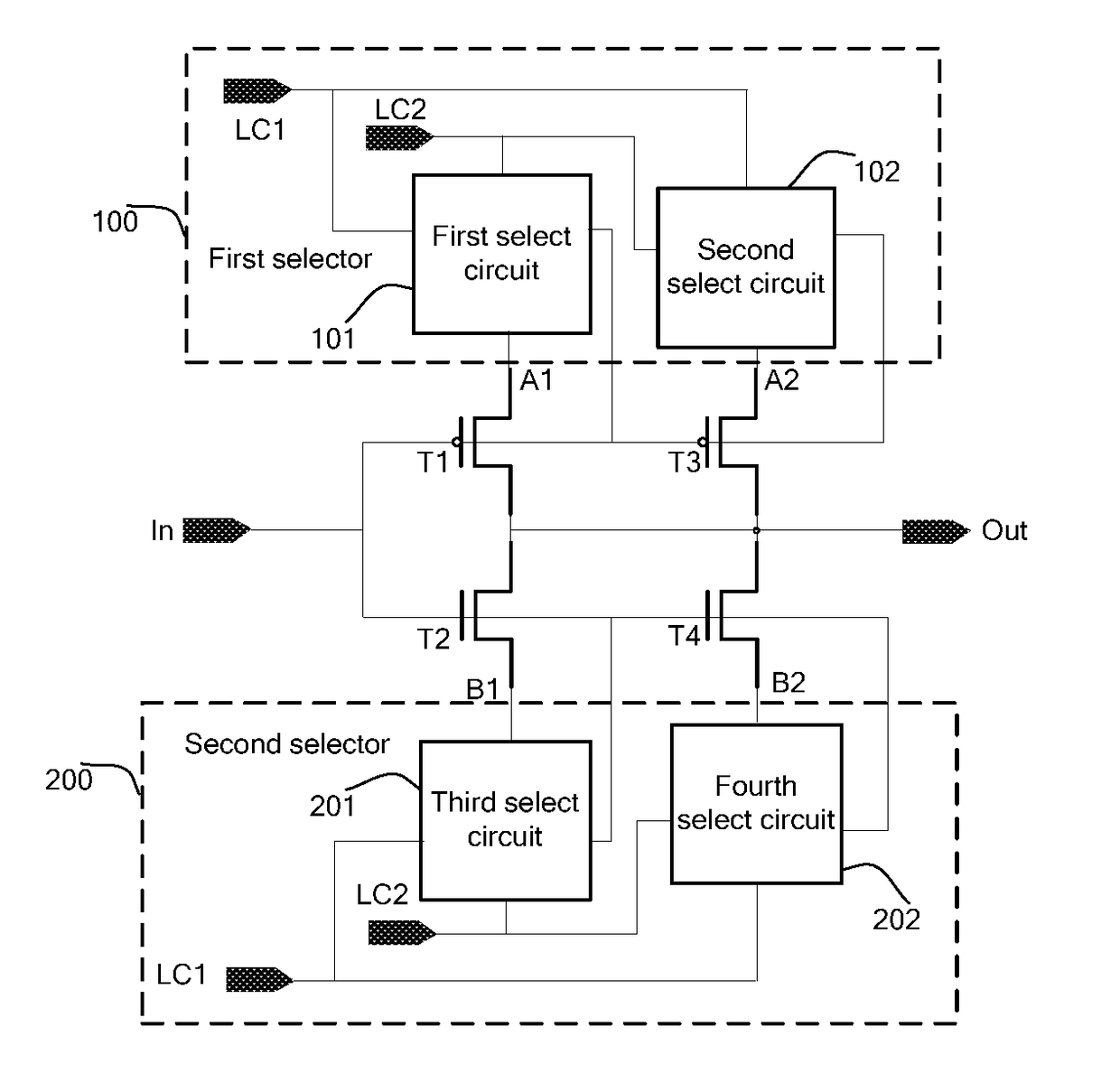
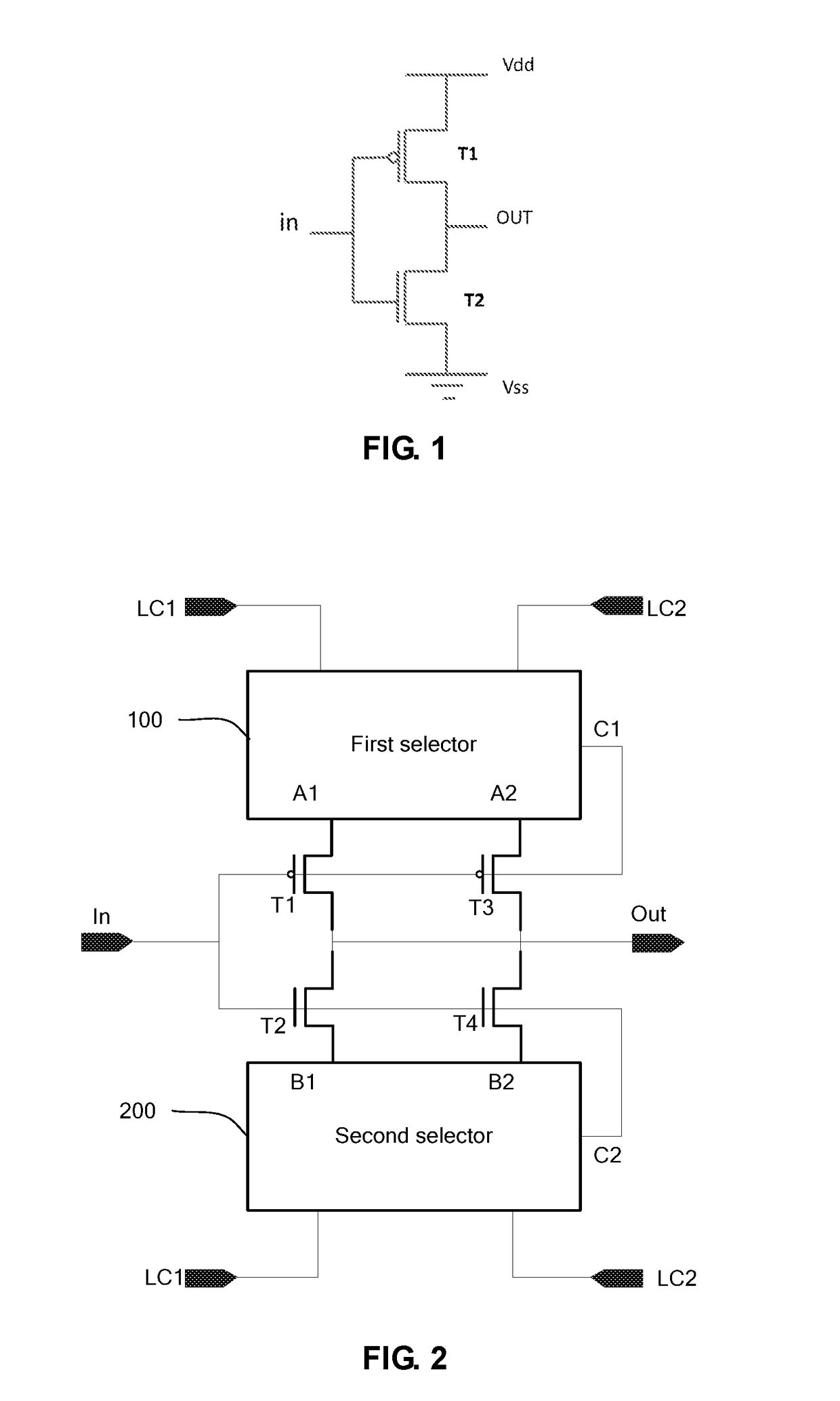
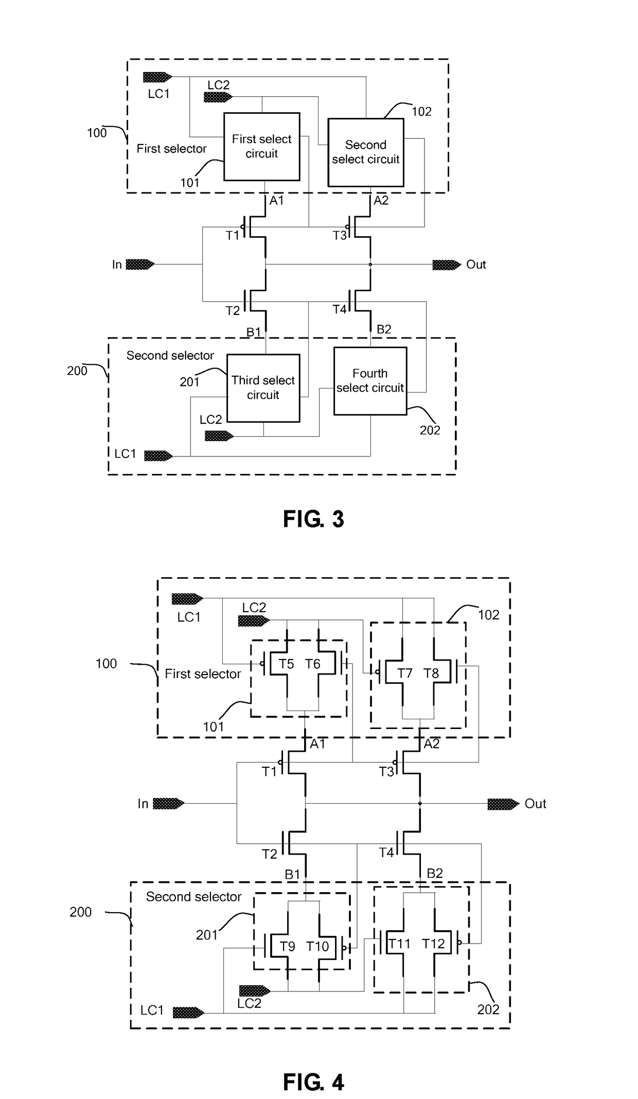
[0032]For better explaining the technical solution and the effect of the present invention, the present invention will be further described in detail with the accompanying drawings in the specific embodiments. It is clear that the described embodiments are part of embodiments of the present application, but not all embodiments. Based on the embodiments of the present invention, all other embodiments to those of ordinary skill in the premise of no creative efforts obtained, should be considered within the scope of protection of the present invention.

[0033]Besides, the following descriptions for the respective embodiments are specific embodiments capable of being implemented for illustrations of the present invention with referring to appended figures. For example, the terms of up, down, front, rear, left, right, interior, exterior, side, etcetera are merely directions of referring to appended figures. Therefore, the wordings of directions are employed for explaining and understanding...


PUM


Abstract

Disclosed is a CMOS inverter, including a first selector, a second selector, and a first transistor, a second transistor, a third transistor and a fourth transistor, which respectively are coupled to the input end of the CMOS inverter through the gates, and all the first transistor, the second transistor, the third transistor and the fourth transistor are coupled to the output end of the CMOS inverter, and sources of the first, the third transistors are respectively and correspondingly coupled to a first output end and a second output end of the first selector, and sources of the second, the fourth transistors are respectively and correspondingly coupled to a first output end and a second output end of the second selector; both the first selector and the second selector receive a first control signal and a second control signal, and both are coupled to the input end.

Description

CROSS REFERENCE[0001]This application claims the priority of Chinese Patent Application No. 201610671927.7, entitled “CMOS inverter and electronic device using the CMOS inverter”, filed on Aug. 16, 2016, the disclosure of which is incorporated herein by reference in its entirety.FIELD OF THE INVENTION[0002]The present invention relates to a circuit technical field, and more particularly relates to a CMOS inverter and an electronic device using the CMOS inverter.BACKGROUND OF THE INVENTION[0003]The CMOS (Complementary Metal Oxide Semiconductor) inverter is an element which is commonly used in the circuit. The CMOS inverter receives an input signal and outputs an output signal which has a logic inversion with the input signal.[0004]Please refer to FIG. 1. FIG. 1 is a circuit structure diagram of the CMOS inverter according to prior art. As shown in FIG. 1, the inverter comprises a P-channel Metal Oxide Semiconductors (PMOS) transistor T1 and a N-channel Metal Oxide Semiconductors (NMO...

Claims


Application Information

Patent Timeline
Patent Type & Authority Applications(United States)
IPC IPC(8): H03K19/0948
CPCH03K19/0948H03K19/20
Inventor JIANG, ZHIXIONG
Owner TCL CHINA STAR OPTOELECTRONICS TECH CO LTD
Why Eureka
Try Eureka