Method of preferential silicon nitride etching using sulfur hexafluoride

a sulfur hexafluoride and silicon nitride technology, applied in the direction of electrical equipment, basic electric elements, electric discharge tubes, etc., can solve the problems of low process margin, high aspect ratio, and extremely difficult control of the fluorocarbon chemistry used for sin etching

Active Publication Date: 2018-07-19
TOKYO ELECTRON LTD
View PDF4 Cites 223 Cited by
  • Summary
  • Abstract
  • Description
  • Claims
  • Application Information

AI Technical Summary

Problems solved by technology

Next generation semiconductor technology development poses a huge challenge as dry etch removal of silicon nitride (SiN) selective to silicon oxide (SiO2) and other materials is needed.
Current fluorocarbon chemistry used for SiN etch becomes extremely difficult to control at narrow mask openings and high aspect ratio due to possibility of clogging of recessed features and the process margin diminishes with each subsequent technology node.

Method used


Image

  • Method of preferential silicon nitride etching using sulfur hexafluoride
  • Method of preferential silicon nitride etching using sulfur hexafluoride
  • Method of preferential silicon nitride etching using sulfur hexafluoride

Examples


Embodiment Construction

[0016]Embodiments of the invention describe substrate processing methods using non-polymerizing chemistry to preferentially etch silicon nitride with high etch selectivity relative to other materials. In one example, SiN / SiO2 etch selectivity greater than 30 can be achieved.

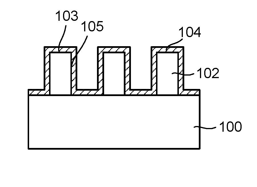
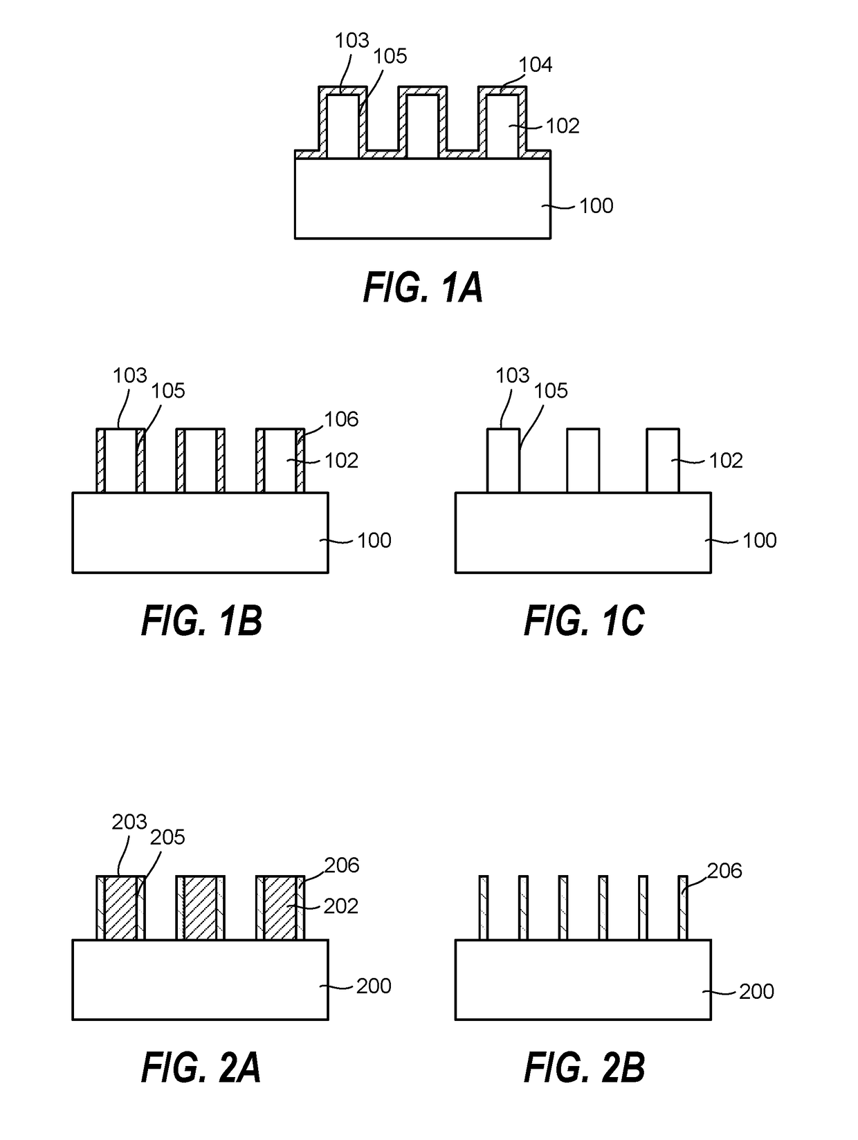
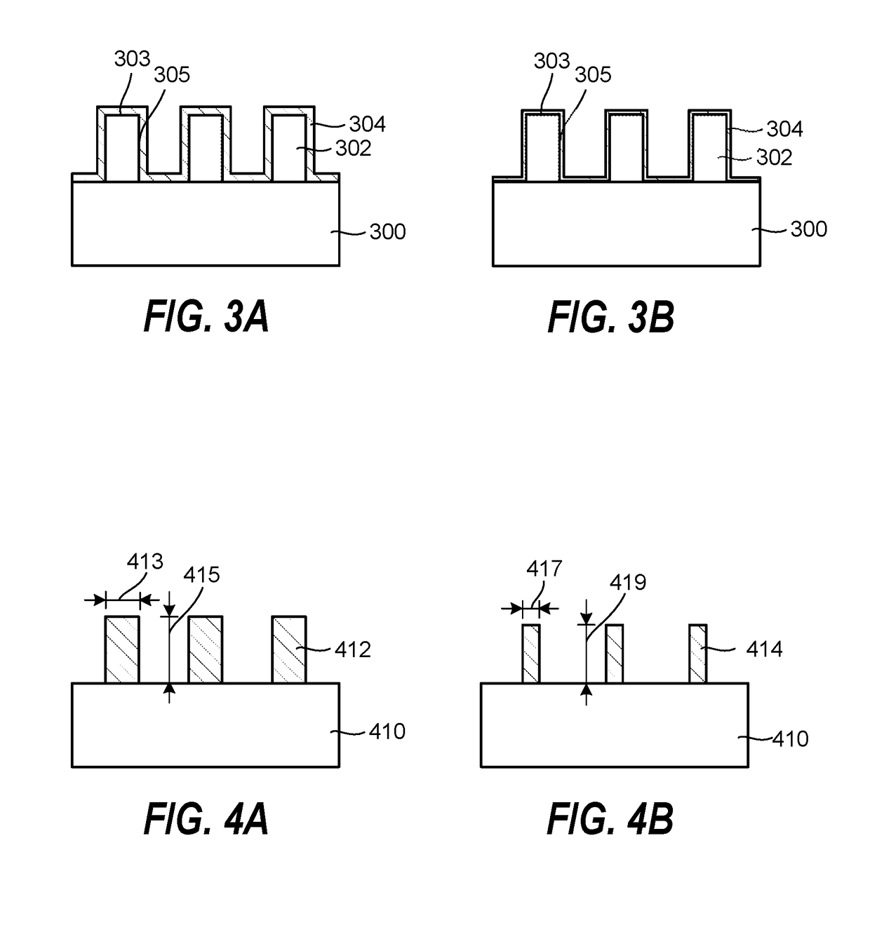
[0017]FIGS. 1A-1C schematically show through cross-sectional views a method of processing a substrate according to an embodiment of the invention. FIG. 1A shows a substrate 100, raised features 102 on the substrate 100, and a SiN spacer layer 104 conformally deposited on the exposed surfaces of the raised features 102 and the substrate 100. In this embodiment, the SiN spacer layer 104 is referred to as a first material, and the raised features 102 are referred to as a second material. The exposed surfaces of the raised features 102 include vertical portions 105 and horizontal portions 103. The substrate 100 and the raised features 102 can, for example, contain or consist of Si or SiO2. In one example, the substra...


PUM

PropertyMeasurementUnit
gas pressureaaaaaaaaaa
RF poweraaaaaaaaaa

Abstract

Embodiments of the invention describe substrate processing methods using non-polymerizing chemistry to preferentially etch silicon nitride relative to other materials found in semiconductor manufacturing. According to one embodiment, a processing method includes providing in a plasma processing chamber a substrate containing a first material containing silicon nitride and a second material that is different from the first material, forming a plasma-excited process gas containing SF6, and exposing the substrate to the plasma-excited process gas to preferentially etch the first material relative to the second material. In one example, the process gas can contain or consist of SF6 and Ar. In another example, the second material is selected from the group consisting of Si and SiO2.

Description

CROSS-REFERENCE TO RELATED APPLICATIONS[0001]This application is related to and claims priority to U.S. Provisional Patent Application Ser. No. 62 / 447,769 filed on Jan. 18, 2017, the entire contents of which are herein incorporated by reference.FIELD OF INVENTION[0002]The present invention relates to the field of semiconductor manufacturing and semiconductor devices, and more particularly, to a method of preferential silicon nitride etching relative to other materials used in semiconductor manufacturing.BACKGROUND OF THE INVENTION[0003]Next generation semiconductor technology development poses a huge challenge as dry etch removal of silicon nitride (SiN) selective to silicon oxide (SiO2) and other materials is needed. Current fluorocarbon chemistry used for SiN etch becomes extremely difficult to control at narrow mask openings and high aspect ratio due to possibility of clogging of recessed features and the process margin diminishes with each subsequent technology node. Hence the n...

Claims


Application Information

Patent Timeline
Patent Type & Authority Applications(United States)
IPC IPC(8): H01L21/311H01L21/67H01J37/32
CPCH01L21/31116H01L21/67069H01J37/3244H01J37/32091H01J2237/334
Inventor SHERPA, SONAM D.RANJAN, ALOK
Owner TOKYO ELECTRON LTD
Why Eureka
Try Eureka