Surface-mounted lc device

a surface-mounted lc device and lc device technology, applied in the field of electromechanical components, can solve the problems of increasing the size of the thin film ipd, generating parasitic inductance components, increasing the loss of radio frequency circuits,

Active Publication Date: 2018-07-26
MURATA MFG CO LTD
View PDF3 Cites 0 Cited by
  • Summary
  • Abstract
  • Description
  • Claims
  • Application Information

AI Technical Summary

Benefits of technology

[0016]In yet another exemplary aspect, preferably, the surface-mounted LC device further includes a second insulating layer covering the planar electrode, and a plurality of terminal electrodes formed on a surface of the second insulating layer and connected to the capacitor and the inductors. With such a feature, since the terminal electrodes are not formed on the side where the thin film inductors are formed, but are formed on the side where the thin film capacitor is formed, the thin film capacitor can be arranged at a shortest distance relative to a circuit formed on a printed wiring board (mounting board), and, therefore, a parasitic inductance can be reduced.
[0021]According to the present exemplary embodiments, the surface-mounted LC device including a plurality of inductors can be obtained in which degradation of Q-values of the individual inductors is suppressed and coupling among the individual inductors is controlled.

Problems solved by technology

However, when the inductor and the capacitor are arranged flush with each other as described in Patent Document 1, for example, it is necessary to increase the substrate area, which therefore unavoidably increases the size of the thin film IPD.
Furthermore, because distances from input / output terminals to the capacitor are increased, a parasitic inductance component generates and, particularly, a loss in a radio frequency circuit increases.
However, when a plurality of coil patterns are formed in a saved space, undesired significant coupling may occur among the coil patterns.

Method used


Image

  • Surface-mounted lc device
  • Surface-mounted lc device
  • Surface-mounted lc device

Examples


Embodiment Construction

[0030]Exemplary embodiments will be described below in connection with several practical examples by referring to the drawings. In the drawings, the same members are denoted by the same reference signs. Although the exemplary embodiments are described in separated forms in consideration of easiness in explanation of principal matters and understanding, individual features of the different embodiments can be partially replaced or combined with each other. In second and subsequent embodiments, explanation of common matters to those in a first embodiment is omitted, and only different points are described. In particular, similar advantageous effects obtained with similar features are not specifically explained in each of the embodiments.

[0031]>

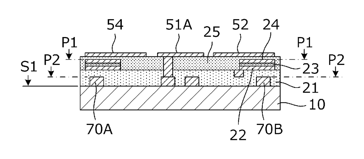
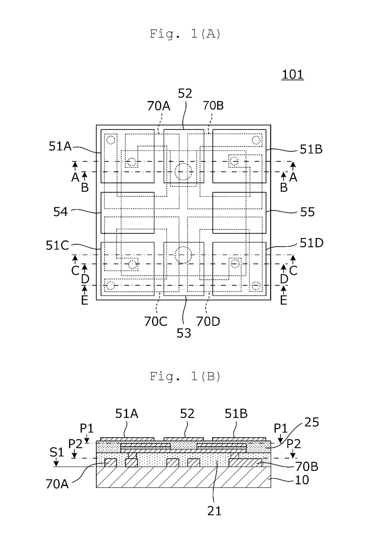
[0032]FIG. 1(A) is a plan view of a surface-mounted LC device 101 according to a first exemplary embodiment, and FIG. 1(B) is a vertical sectional view taken along a line A-A in FIG. 1(A). In the exemplary aspect, a surface appearing in FIG. 1(A)...


PUM

PropertyMeasurementUnit
currentsaaaaaaaaaa
currentsaaaaaaaaaa
currentaaaaaaaaaa

Abstract

A surface-mounted LC device that includes a substrate having a first surface, multiple inductors formed on the first surface and formed respectively by multiple coiled conductor patterns, a first insulating layer covering the multiple coiled conductor patterns, and a capacitor that is formed on the first insulating layer by a planar electrode. Moreover, the planar electrode covers first zones in which portions of the coiled conductor patterns are adjacent to each other and current directions are opposite to each other in a plan view of the surface-mounted LC device.

Description

CROSS REFERENCE TO RELATED APPLICATIONS[0001]The present application is a continuation of PCT / JP2016 / 078553 filed Sep. 28, 2016, which claims priority to Japanese Patent Application No. 2015-196393, filed Oct. 2, 2015, the entire contents of each of which are incorporated herein by reference.TECHNICAL FIELD[0002]The present disclosure relates generally to an electronic component including an inductor and a capacitor, and, more particularly, to a surface-mounted LC device that is suitable for reduction of size and thickness.BACKGROUND[0003]Currently, there is a thin film IPD (Integrated Passive Device) in which an inductor and a capacitor are integrally formed on a silicon substrate, an alumina substrate, or the like by a thin film process. Such existing IPD designs are generally disclosed in Patent Documents 1 and 2 (identified below).[0004]For example, Patent Document 1 discloses a technique of, in a step of fabricating a thin film circuit, forming a dielectric film for a thin film...

Claims


Application Information

Patent Timeline
Patent Type & Authority Applications(United States)
IPC IPC(8): H01F27/40H01F27/28H01G4/40H03H1/00H03H7/01
CPCH01F27/40H01F27/2804H01G4/40H03H1/00H03H7/0115H03H2001/0021H01F17/0013H01F2027/348H03H2001/0085H01L27/016H01L28/10H01L28/40H05K1/113H05K1/162H05K1/165
Inventor ISHIZUKA, KENICHIYAZAKI, HIROKAZU
Owner MURATA MFG CO LTD
Why Eureka
Try Eureka