Semiconductor laser device

a laser device and semiconductor technology, applied in the direction of semiconductor lasers, lasers, solid-state devices, etc., can solve the problems of large deterioration of light waveform, and difficulty in demodulating signals, so as to reduce parasitic inductance, reduce the use of wires, and improve the effect of light waveform modulation

Pending Publication Date: 2022-07-14
MITSUBISHI ELECTRIC CORP
View PDF0 Cites 0 Cited by
  • Summary
  • Abstract
  • Description
  • Claims
  • Application Information

AI Technical Summary

Benefits of technology

[0009]According to the present application, not only a parasitic inductance can be reduced by reducing usage of t

Problems solved by technology

At this time, even though the signal input to the LD chip is an ideal square wave, a large impedance mismatch occurs due to parasitic inductances of the wires and the leads, whereby the modulated light waveform of the laser light emitted from the LD chip has a longer rise time and a longer fall time, thus resulting in deterioration of th

Method used


Image

  • Semiconductor laser device
  • Semiconductor laser device
  • Semiconductor laser device

Examples


embodiment 1

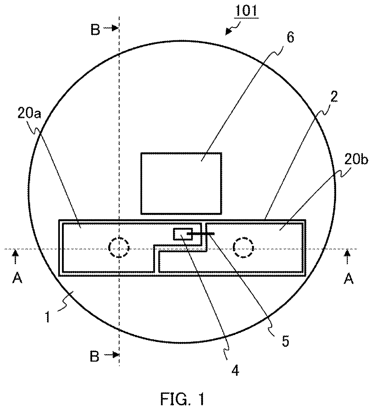
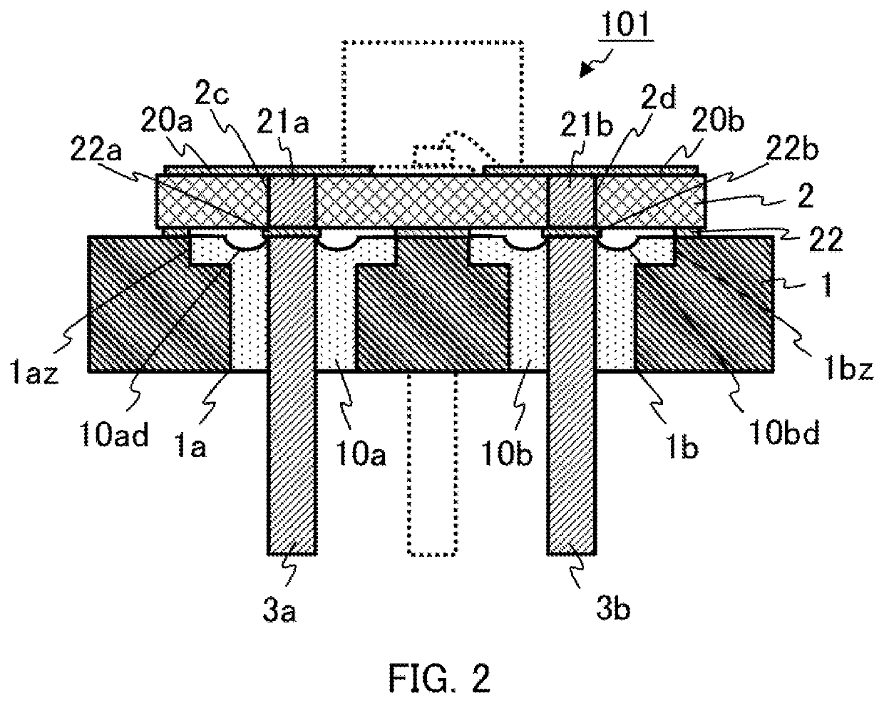
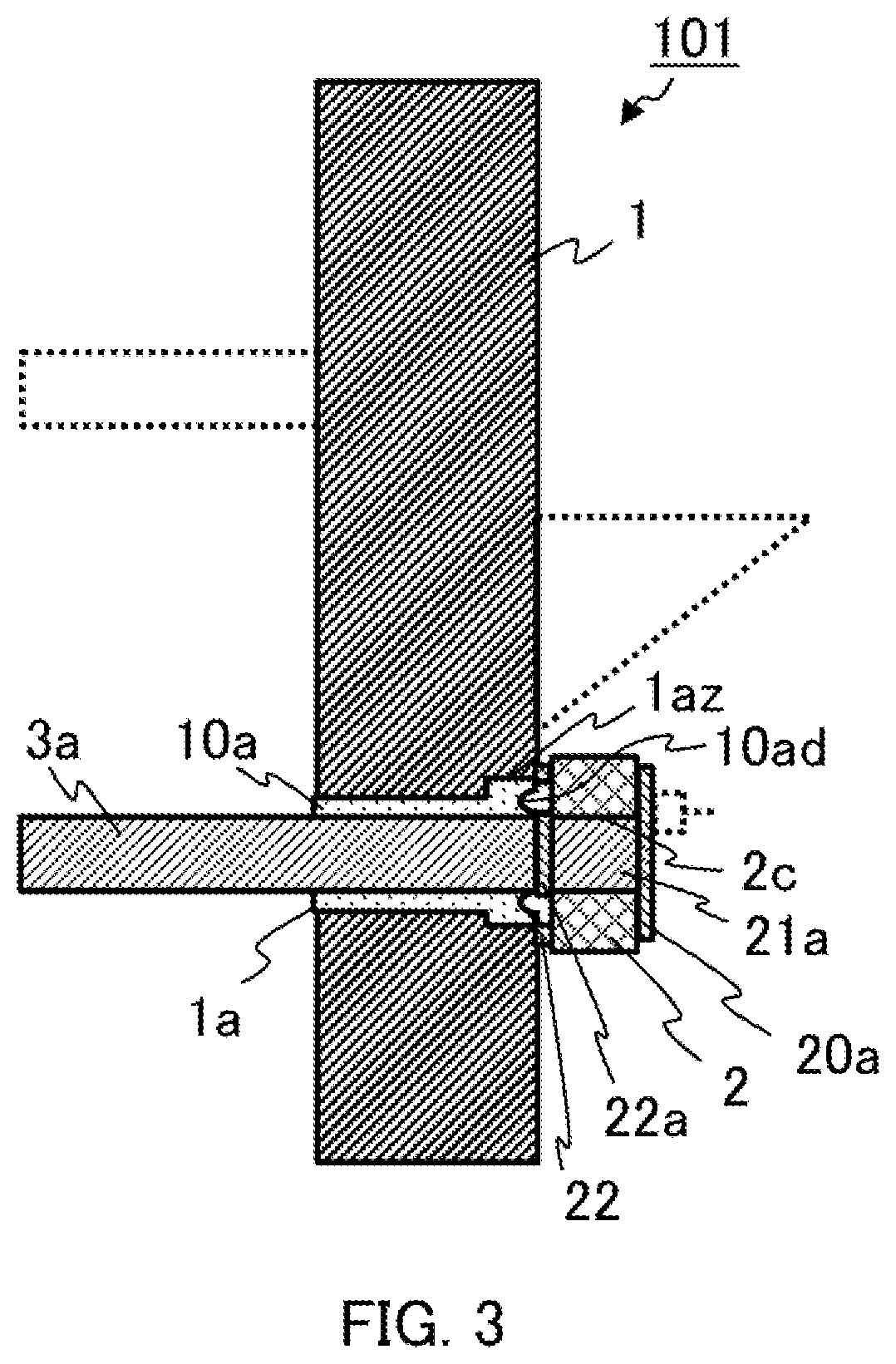
[0022]FIG. 1 is a plan view showing a configuration of a semiconductor laser device 101 according to Embodiment 1 of the present application. FIG. 2 is a sectional view taken in the direction of the arrows along the line A-A of FIG. 1, and FIG. 3 is a sectional view taken in the direction of the arrows along the line B-B of FIG. 1. With reference to FIG. 1 to FIG. 3, the semiconductor laser device 101 comprises a stem 1 serving as a base; an LD submount 2 mounted on the surface of the stem 1; leads 3a, 3b fixed in the through holes 1a, 1b formed in the stem 1 and electrically connected to surface electrodes 20a, 20b on the LD submount 2 via conductive embedded layers 21a, 21b in via holes 2c, 2d and back electrodes 22a, 22b, respectively; an LD chip 4, which is a semiconductor laser element, joined to the surface of the surface electrode 20a on the LD submount 2; a gold wire 5 connecting the top surface electrode of the LD chip 4 to the surface electrode 20b; and a mirror 6 for refl...

embodiment 2

[0033]While Embodiment 1 described the case of connecting the surface electrodes 20a, 20b to the leads 3a, 3b via the embedded layers 21a, 21b in the via holes 2c, 2d, Embodiment 2 describes a case of connecting the surface electrodes 20a, 20b with the leads 3a, 3b by direct contact.

[0034]FIG. 5 is a plan view showing a configuration of a semiconductor laser device 102 according to Embodiment 2 of the present application. FIG. 6 is a sectional view taken in the direction of arrows along the line A-A of FIG. 5. As shown in FIGS. 5 and 6, the semiconductor laser device 102 has leads 3a, 3b that protrude from the surface of the stem 1 into direct contact with surface electrodes 70a, 70b on an LD submount 7 that is formed by cutting two corners of the LD submount 2 used in Embodiment 1, to be electrically connected with the surface electrodes 70a, 70b by soldering without via the embedded layers in the via holes, respectively. The top ends of the leads 70a, 70b may be expanded or constr...

embodiment 3

[0038]Embodiment 3 describes a case of mounting a PD chip for monitoring the output of the laser light emitted from the LD chip 4.

[0039]FIG. 9 is a plan view showing a configuration of a semiconductor laser device 103 according to Embodiment 3 of the present application. FIG. 10 is a sectional view taken in the direction of arrows along the line B-B of FIG. 9.

[0040]In general semiconductor laser devices, an LD chip is mounted so as to emit its laser light in the direction perpendicular to the stem without using a mirror, and a PD chip is implemented perpendicularly to the LD chip (parallel to the stem) to receive a light leaking from the rear side of the LD chip in order to monitor the output of the laser light. However, it is difficult to ensure a space for mounting the PD chip perpendicularly to and behind the LD chip 4 in the configuration of Embodiment 1.

[0041]Hence, as shown in FIGS. 9 and 10, the semiconductor laser device 103 has a PD chip 9, which is a photodiode element, an...


PUM


Abstract

A semiconductor laser device comprises a stem serving as a base; a laser diode LD submount having surface electrodes arranged thereon and joined to the surface of the stem; an LD chip joined to the surface electrode and connected with the surface electrode; and leads fixed in through holes formed in the stem by means of sealing parts and electrically connected to the surface electrodes via embedded layers in via holes formed in the LD submount, wherein grooves are formed in portions of the sealing parts or in portions of the LD submount around the connections between the leads and the embedded layers, to obtain a good modulated light waveform.

Description

TECHNICAL FIELD[0001]The present application relates to a semiconductor laser device.BACKGROUND ARTS[0002]In a conventional semiconductor laser device, a laser diode chip (abbreviated as “LD chip” hereinafter) is implemented on a heatsink that perpendicularly protrudes from a metal base of a stem (see, for example, Patent Document 1). Furthermore, a semiconductor laser device is known that comprises a submount on a stem and a semiconductor laser element mounted on the submount for emitting a laser light parallel to the stem (see, for example, Patent Document 2).[0003]A conventional semiconductor laser device receives a modulation signal superimposed on a direct current (DC) bias to drive the LD chip. The modulation signal is input to the LD chip via a gold wire and the submount to turn the laser light on and off in response to on and off of the square modulation signal. At this time, even though the signal input to the LD chip is an ideal square wave, a large impedance mismatch occu...

Claims


Application Information

Patent Timeline
IPC IPC(8): H01S5/0232H01S5/026
CPCH01S5/0232H01S5/0262H01S5/02212H01S5/0237H01S5/02345H01S5/06226H01L24/00H01S5/02255H01S5/0239H01S5/0683H01L2224/48091H01L2924/19107H01L2224/45144H01L24/45H01L24/48H01L2924/12042H01L2924/12043H01L2924/181H01L2924/15312H01L2224/48227H01L2924/00014H01L2924/00012
Inventor KOSAKA, NAOKIFUCHIDA, AYUMISHIMADA, MASAAKISAKAINO, GOTAKASE, TADASHI
Owner MITSUBISHI ELECTRIC CORP
Why Eureka
Try Eureka