Semiconductor structure and manufacturing method thereof

Active Publication Date: 2018-07-26
WINBOND ELECTRONICS CORP
View PDF0 Cites 0 Cited by
  • Summary
  • Abstract
  • Description
  • Claims
  • Application Information

AI Technical Summary

Benefits of technology

[0009]In light of the foregoing, the present disclosure adopts the 3-D printing technique to &tin a plurality of conductive bumps on the chip and the substrate respectively. Then, a FPC board is configured to connect between the chip and the substrate, such that the conductive bumps on the chip and the substrate penetrate through two opposite ends of the FPC board respectively to electrically connect the chip and the substrate through the FPC board. With such configuration, the electrical connection between th

Problems solved by technology

However, there are still problems in the conventional wire-bonding technique.
For example, a short circuit may occur between adjacent metal wires which are intended to be isolated, and an open circuit may abnormally occur in one metal wire or between more metal wires which are intended to be connected to each other.
For example, movement of the metal wires during manufacturing process such as sway, sweep, etc., may lead to short circuit between the adjacent metal wires which are intended to be isolated.
More severely, such movement of the metal wires may

Method used


Image

  • Semiconductor structure and manufacturing method thereof
  • Semiconductor structure and manufacturing method thereof
  • Semiconductor structure and manufacturing method thereof

Examples


Example

[0012]The present disclosure will now be described more fully with reference to the accompanying drawings, in which exemplary embodiments of the disclosure are shown. The terms used herein such as “above”, “below”, “front”, “back”, “left” and “right” are for the purpose of describing directions in the figures only and are not intended to be limiting of the disclosure. Moreover, in the following embodiments, the same or similar devices are denoted by the same or similar referential numbers.

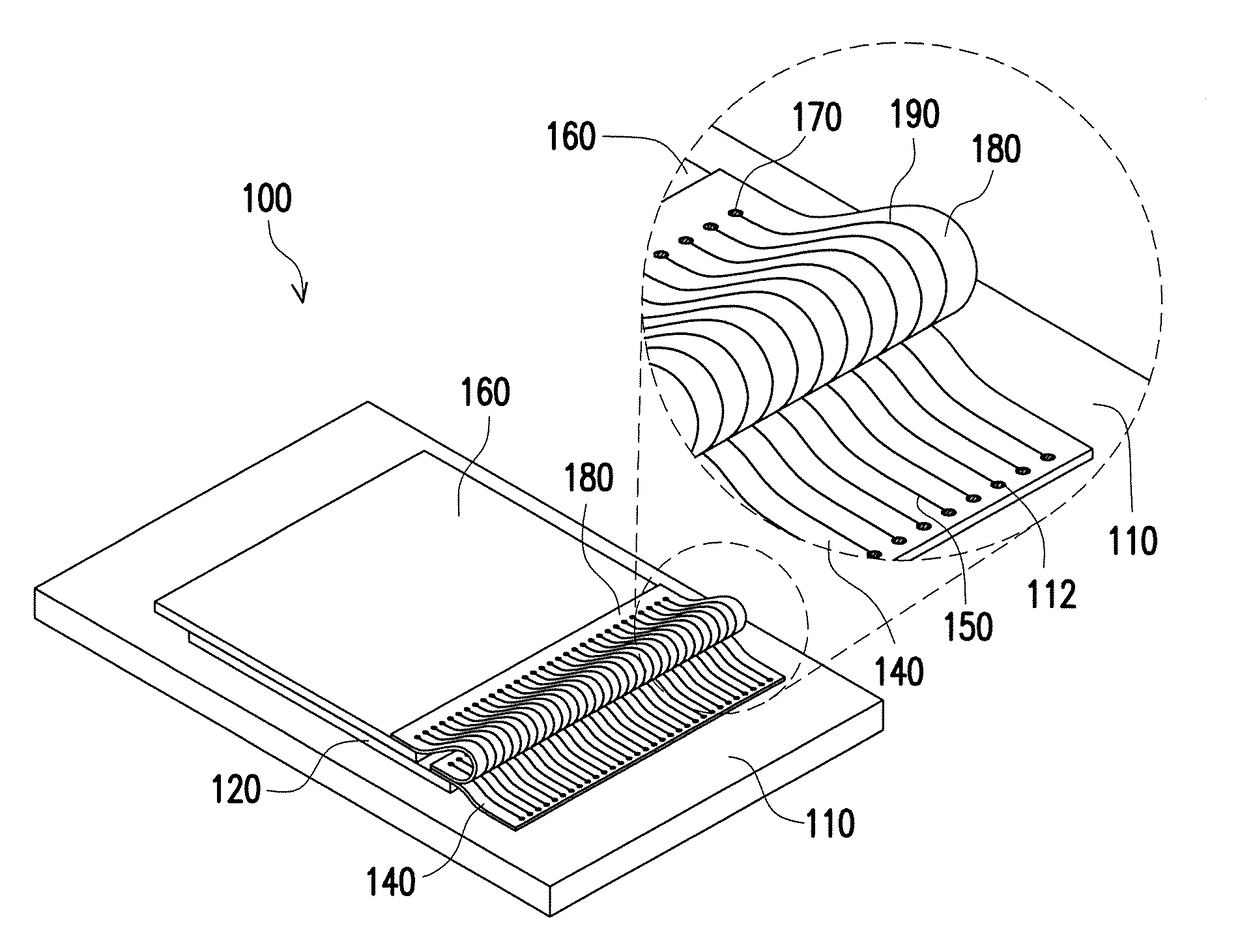
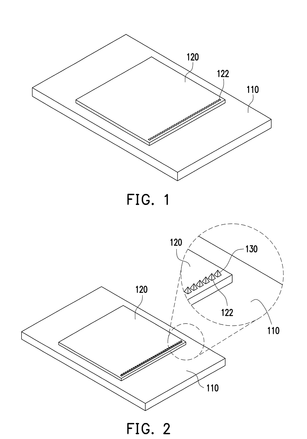
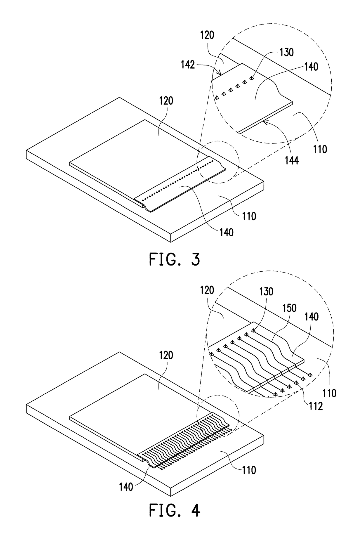
[0013]FIG. 1 to FIG. 7 illustrates a manufacturing process of a semiconductor structure according to an embodiment of the present disclosure. In the present embodiment, the manufacturing method of the semiconductor structure 100 includes the following steps. First, a substrate as shown in FIG. 1 is provided. Next, a first chip 120 is disposed on the substrate 110. In the present embodiment, the first chip 120 may be obtained by dicing a wafer having a plurality of chips. The first chip 120 includes...


PUM


Abstract

A semiconductor structure includes a substrate, a chip, a plurality of conductive bumps, a flexible printed circuit (FPC) board and a plurality of circuit patterns. The chip is disposed on the substrate and includes a plurality of pads. The conductive bumps are disposed on the pads respectively. The FPC board is connected between the substrate and the chip, and the conductive bumps penetrate through an end of the FPC board. The circuit patterns are disposed on the FPC board and electrically connected to the conductive bumps and the substrate.

Description

CROSS-REFERENCE TO RELATED APPLICATION[0001]This application claims the priority benefit of China application serial no. 201710060906.6, filed on Jan. 25, 2017. The entirety of the above-mentioned patent application is hereby incorporated by reference herein and made a part of this specification.BACKGROUNDTechnical Field[0002]The present disclosure generally relates to a semiconductor structure and manufacturing method thereof. More particularly, the present disclosure relates to a semiconductor structure and manufacturing method thereof with higher yield.Description of Related Art[0003]In an information-explosion world, ICs are widely used in the daily life, including entertainment, education, transportation and households. With the rapid progress in electronic technologies, more personalized and functionally powerful electronic products are out in the market. In general, an electronic product controls its own operation through at least one chip, and the chip may be electrically co...

Claims


Application Information

Patent Timeline
IPC IPC(8): H01L23/00H01L25/065H01R4/2407H01R12/62
CPCH01L24/50H01L25/0657H01L24/13H01R4/2407H01R12/62H01L2225/06562H01L2224/13016H01L2224/13139H01L2224/13124H01L23/50H01L24/89H01L2224/89H01L23/4985H01L2225/06579H01L2224/32145H01L2224/32225H01L2224/73219H01L2224/73269
Inventor CHEN, YU-MING
Owner WINBOND ELECTRONICS CORP
Why Eureka
Try Eureka