
Method for producing a thin film transistor and a device of the same

Inactive Publication Date: 2009-05-14
TAIWAN TFT LCD ASSOC +6
View PDF5 Cites 0 Cited by
  • Summary
  • Abstract
  • Description
  • Claims
  • Application Information

AI Technical Summary

Benefits of technology

[0014]The primary objective of the invention is therefore to specify a thin film transistor that can replace the conventional semiconductor process with simple steps, thereby improving manufacturing efficiency and saving on production costs.
[0015]The secondary objective of the invention is therefore to specify a thin film transistor that can adjust the depth of a desired pattern directly, without additional etching or other processes.

Problems solved by technology

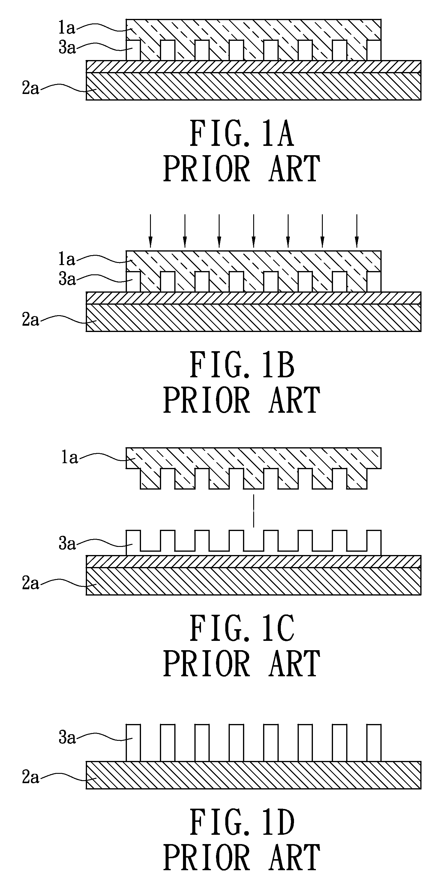
As such, semiconductor technology, which consumes a lot of time and labor and requires expensive paraphernalia, is often criticized.
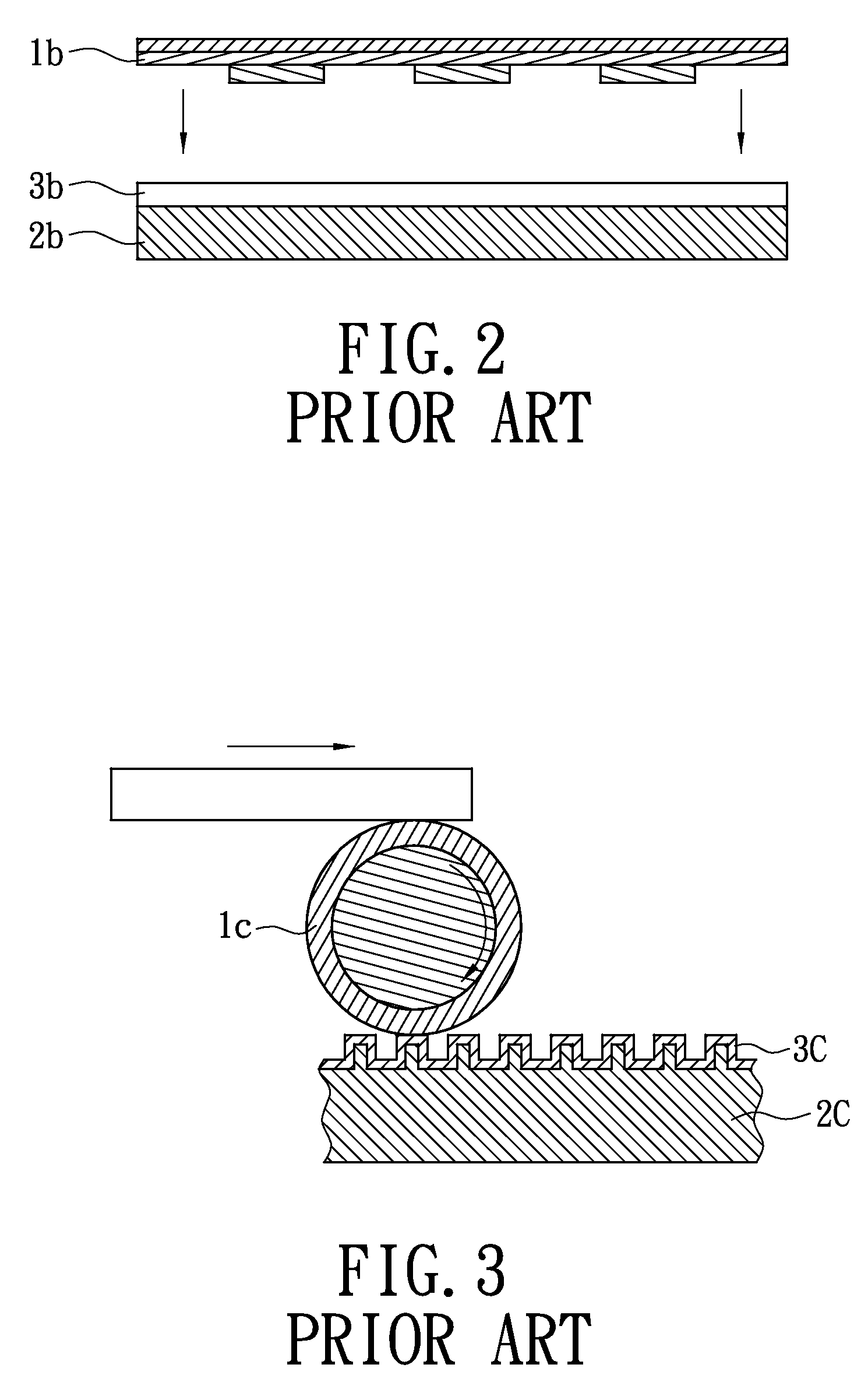
This method however, lacks a precise and stable alignment.
Furthermore, the mold 1c is made of Polydimethylsiloxane (PDMS) that wears out easily, deforms and has a negative effect on the precision of the pattern thereof.
The impression mold however, often suffers from defective patterns due to the resilient property caused by the pressure that it experiences in the pressing step.
So the pattern is often imprecise.

Method used


Image

  • Method for producing a thin film transistor and a device of the same
  • Method for producing a thin film transistor and a device of the same
  • Method for producing a thin film transistor and a device of the same

Examples


Embodiment Construction

[0029]The present invention produces a plurality of ladder opaque protrusions on a transparent mold plate, and then presses the transparent mold plate onto a substrate that has a positive photosensitive coating formed in advance. a part of the positive photosensitive coating is explored via a UV light, thus removing the unshielded part via a chemical solvent, and the other part of the positive photosensitive coating shielded under the ladder opaque protrusion is defined the different depth on the predetermined pattern, thereby, defining both a predetermined pattern and different depth of the predetermined pattern simultaneously without additional etching or other processes.

[0030]The method according to the present invention can be brought into practice to each layer of a thin film transistor by taking different photosensitive materials with specific properties; for example, a semiconductor photosensitive material can be used as a semiconductor layer and the like, such as active laye...


PUM

PropertyMeasurementUnit
Adhesion strengthaaaaaaaaaa
Metallic bondaaaaaaaaaa
Transparencyaaaaaaaaaa

Abstract

A method for producing a thin film transistor and including the following steps for preparing a glass substrate; having a positive photosensitive coating on the glass substrate; providing a transparent mold plate, having a plurality of ladder opaque protrusions in accordance with a predetermined pattern having different depth; controlling the transparent mold plate downwardly to press into the positive photosensitive coating and non-contacting to the glass substrate; exploring a part of the positive photosensitive coating via an explosion by a UV light; remaining the other part of the positive photosensitive coating, which is shielded by the protrusions and shaped corresponding to the predetermined pattern; separating the transparent mold plate from the glass substrate, and removing the other parts of the photosensitive coating unshielded via a chemical solvent. Thereby, after the positive photosensitive coating is pressed, cured, and cleaned the thin film transistor is formed.

Description

[0001]This application is a Continuation-in-Part of application Ser. No. 10 / 995,479, filed 24 Nov. 2004, and entitled Method for producing a thin film transistor and a device of the same.BACKGROUND OF THE INVENTION[0002]1. Field of the Invention[0003]The present invention relates to a method for producing a thin film transistor, and particularly relates to a method, rather than a semiconductor process, for producing a thin film transistor.[0004]2. Background of the Invention[0005]A conventional method for producing a conventional thin film transistor uses semiconductor technology, which includes film deposition, photolithography technology, etching processes and the like. The film deposition process includes deposing a film of dielectric or insulating material by chemical vapor deposition (CVD) and deposing a film of electric material by physical vapor deposition (PVD). The photolithography and the etching processes define a pattern thereof. The equipment used for film deposition, p...

Claims


Application Information

Patent Timeline
IPC IPC(8): H01L27/12G03F7/20
CPCB82Y10/00B82Y40/00G03F7/0002H01L27/1292H01L51/0022H01L27/1288H01L29/66742H10K71/611
Inventor CHOU, LIN-ENTSAI, CHIA-HAOWANG, WEN-TUNG
Owner TAIWAN TFT LCD ASSOC
Learn More