Image sensor and image capturing apparatus
a technology which is applied in the field of image sensor and image capturing apparatus, can solve the problems of image quality degradation and image quality degradation, and achieve the effect of favorable image and suppressing field curvatur
- Summary
- Abstract
- Description
- Claims
- Application Information
AI Technical Summary
Benefits of technology
Problems solved by technology
Method used
Image

Examples
first embodiment
[0030]The following describes an embodiment of the present invention when applied to an image sensor used in an image capturing apparatus such as a digital single-lens reflex camera or a video camera. Note that the present invention is also applicable to other apparatuses that are equipped with an image sensor whose imaging plane has a curved shape.
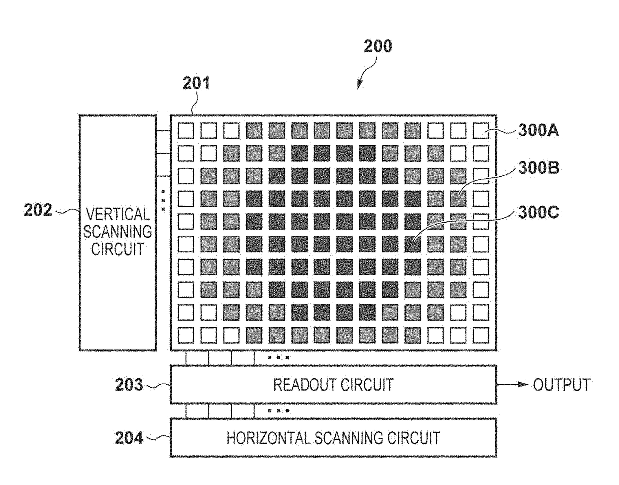
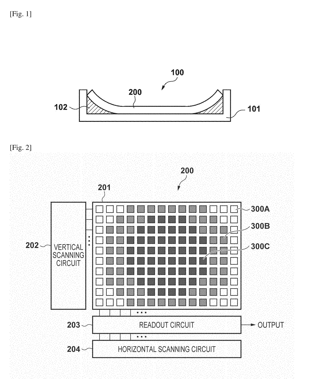
[0031]First, a description is given of a schematic configuration of the image sensor according to the first embodiment of the present invention with reference to FIG. 1. An image sensor 100 includes a CMOS semiconductor substrate. An imaging semiconductor substrate 200, on which a plurality of pixels are two-dimensionally arranged, is supported on a supporting substrate 101 having a recessed shape. The imaging semiconductor substrate 200 has a curved shape in which a peripheral portion is raised as shown in the drawing. The gap between the supporting substrate 101 and the imaging semiconductor substrate 200 is filled with an adhesive 102,...
second embodiment
[0063]The magnitude of stress generated within the imaging plane of an imaging semiconductor substrate having a curved shape varies depending on the curved shape and the manufacturing method. The present embodiment provides a description of an example where the present invention is applied to an imaging semiconductor substrate having a curved shape that is different from the curved shape in the first embodiment.
[0064]First, a description is given of a schematic configuration of an image sensor according to the second embodiment with reference to FIG. 7.
[0065]An image sensor 700 includes a CMOS semiconductor substrate. An imaging semiconductor substrate 800, on which a plurality of pixels are two-dimensionally arranged, is supported on a supporting substrate 701 having a recessed shape. The imaging semiconductor substrate 800 has a spherical shape, and does not have a flat portion in a central region thereof. The gap between the supporting substrate 701 and the imaging semiconductor ...
third embodiment
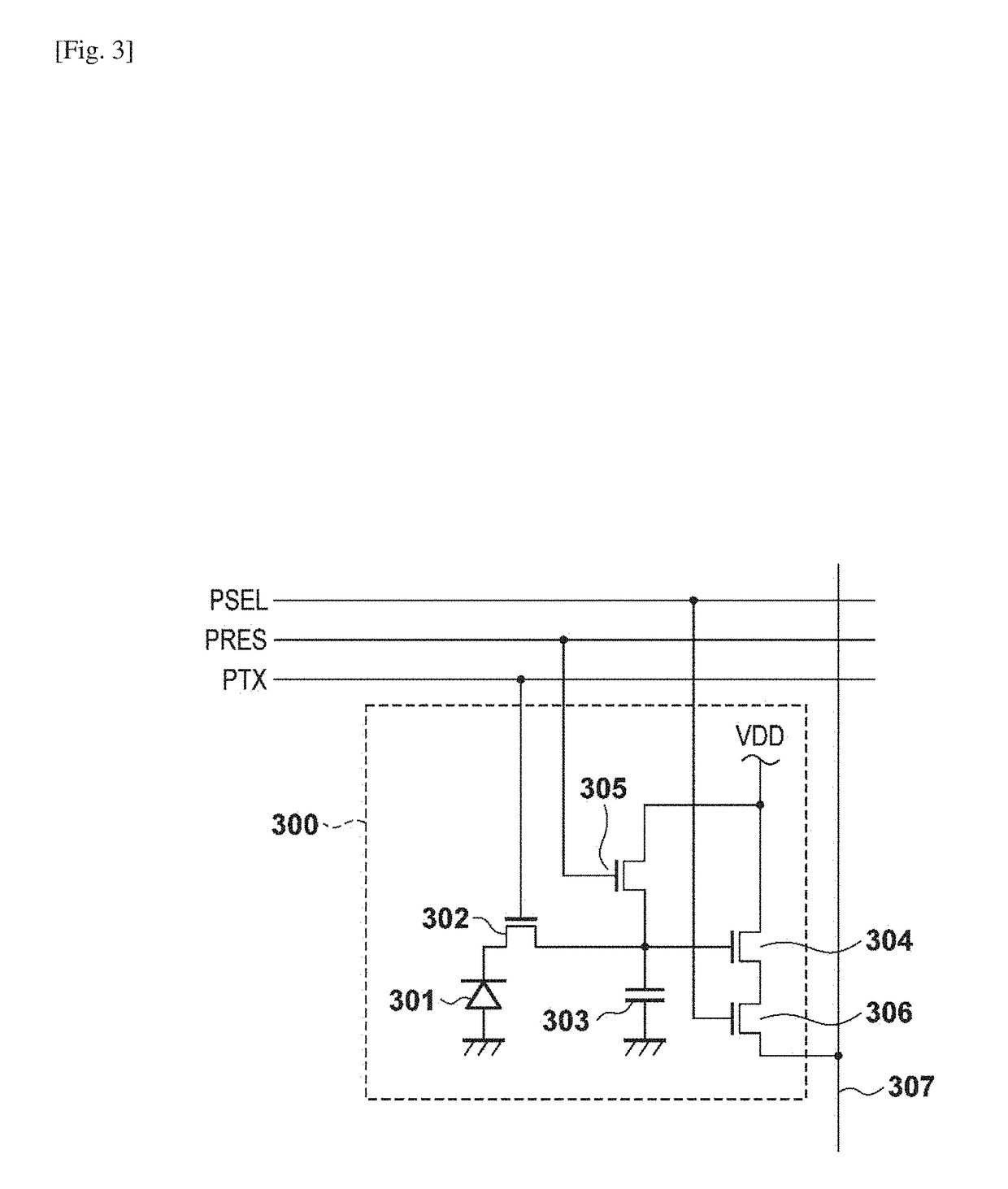
[0071]As in the above-described first and second embodiments, if the degrees of impurity concentration in the dark current suppression regions 404A to 404C that are of the conductivity type opposite to the conductivity type of the photodiodes 301 are set to be high, electric charge collection in the vicinity of the surfaces of the photodiodes 301 is hindered, and the spectral sensitivity of the photodiodes 301 changes. As a result, in the image sensor having the R, G and B color filters, the color ratios of the R, G, and B colors differ between the dark current suppression regions in which the degrees of impurity concentration are different from each other. In light of this problem, the third embodiment describes a configuration in which a spectral sensitivity correction unit that corrects changes in the spectral sensitivity is provided in an image capturing apparatus 900 in which the image sensor 100 according to the first embodiment or the image sensor 700 according to the second ...
PUM
 Abstract
Description
Claims
Application Information
 - R&D
- Intellectual Property
- Life Sciences
- Materials
- Tech Scout
- Unparalleled Data Quality
- Higher Quality Content
- 60% Fewer Hallucinations
Browse by: Latest US Patents, China's latest patents, Technical Efficacy Thesaurus, Application Domain, Technology Topic, Popular Technical Reports.
© 2025 PatSnap. All rights reserved.Legal|Privacy policy|Modern Slavery Act Transparency Statement|Sitemap|About US| Contact US: help@patsnap.com