Piezoelectric sensor and piezoelectric device

a piezoelectric device and piezoelectric sensor technology, applied in the field of piezoelectric sensors and piezoelectric devices, can solve the problems of decreasing piezoelectric devices, and reducing the degree of integration, and achieve the effect of increasing the degree of integration of the transmitting piezoelectric element and the receiving piezoelectric elemen

Active Publication Date: 2018-08-09
SEIKO EPSON CORP
View PDF0 Cites 12 Cited by
  • Summary
  • Abstract
  • Description
  • Claims
  • Application Information

AI Technical Summary

Benefits of technology

[0008]An advantage of some aspects of the invention is to provide a piezoelectric sensor and a piezoelectric device capable of increasing the degree of integration of a transmitting piezoelectric element and a receiving piezoelectric element.

Problems solved by technology

In addition, in the proximity ultrasonic sensor in JP-A-2011-82624, since the ultrasonic transducer for transmission and the ultrasonic transducer for reception are integrally arranged adjacent to each other in a direction which suppresses the reverberation vibrations, there is a problem in that the degree of integration decreases.
Furthermore, in the piezoelectric thin film resonator of JP-A-2009-284021, since elements specialized for transmission and reception are not used and various signals are transmitted and received within the same element, in a case where another circuit such as, for example, a feedback circuit is provided separately, there is a problem in that the degree of integration decreases.
Here, such a problem similarly exists in all piezoelectric devices on which a piezoelectric sensor is mounted.

Method used


Image

  • Piezoelectric sensor and piezoelectric device
  • Piezoelectric sensor and piezoelectric device
  • Piezoelectric sensor and piezoelectric device

Examples


first embodiment

Ultrasonic Probe

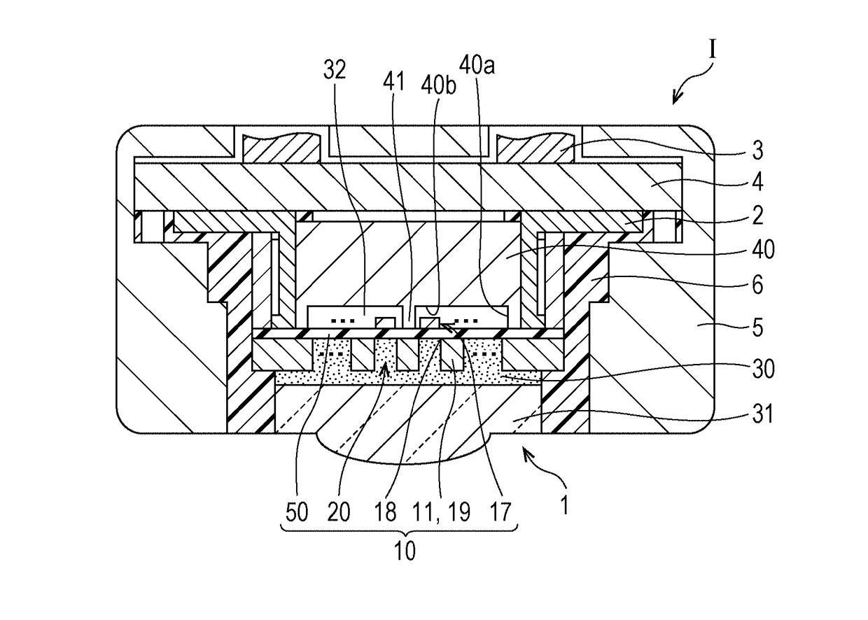
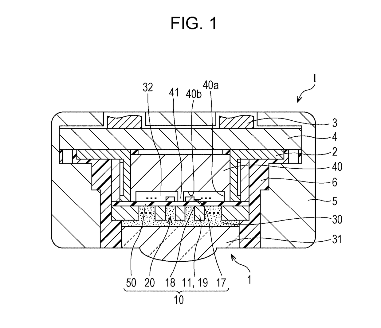
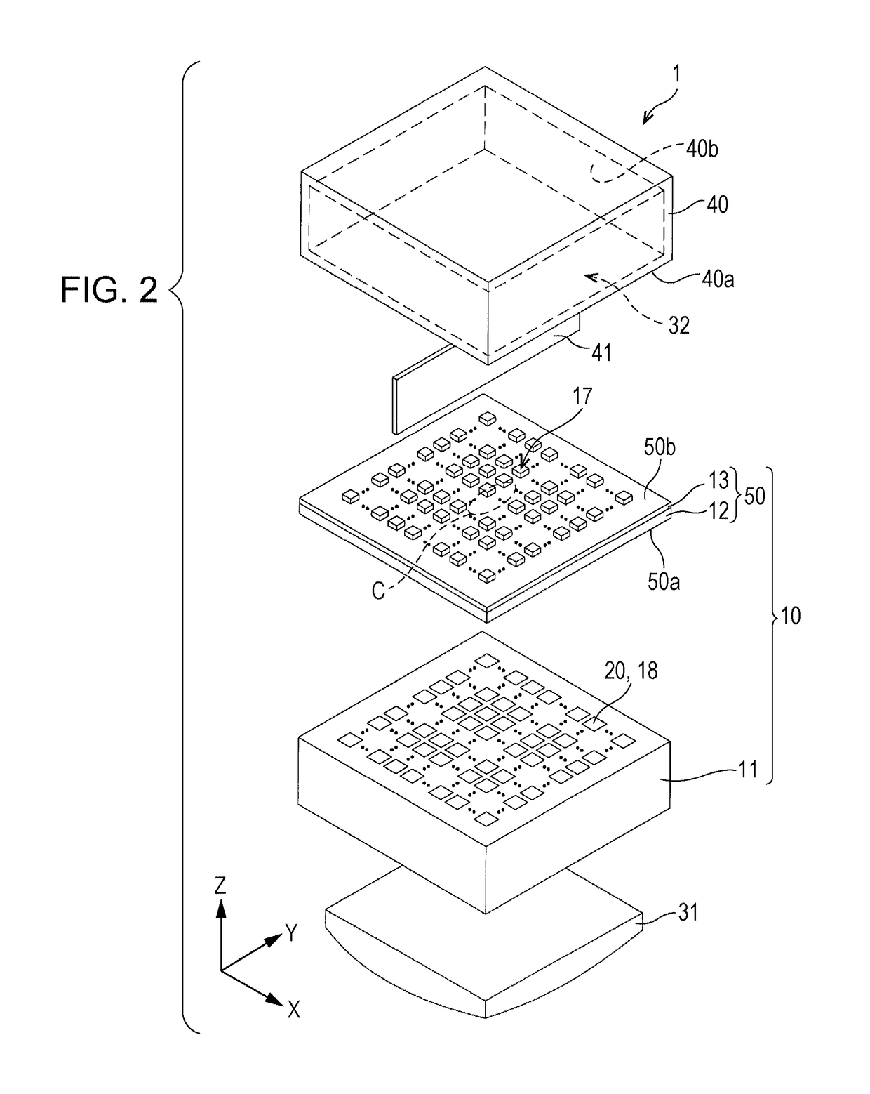
[0044]In the first embodiment, an ultrasonic probe is taken as an example of an ultrasonic device which is a piezoelectric device, and description will be given thereof with reference to the drawings. FIG. 1 is a cross-sectional view showing a configuration example of an ultrasonic probe according to the first embodiment. As shown in the diagram, an ultrasonic probe (probe) I is formed to be provided with an ultrasonic sensor 1 of a type (CAV surface type) in which the side opposite to the piezoelectric element 17 of the vibrating plate 50 is an ultrasonic wave passage region, a flexible printed circuit board (FPC board) 2 connected to the ultrasonic sensor 1, a cable 3 drawn out from an apparatus terminal (not shown), a relay board 4 for relaying the FPC board 2 and the cable 3, a housing 5 for protecting the ultrasonic sensor 1, the FPC board 2, and the relay board (FPC board) 4, and a waterproof resin 6 filled between the housing 5 and the ultrasonic sensor 1. In ...

second embodiment

Ultrasonic Sensor

[0129]The ultrasonic sensor 1 of the present embodiment is the same ultrasonic sensor as the first embodiment except that the configuration of the piezoelectric element 17 and the opening 18 (space 20) of the first embodiment is changed. Accordingly, in the present embodiment, a description will be given of mainly the configuration of the piezoelectric element and the opening (space), and explanation of other configurations will be omitted as appropriate. FIG. 7 is a plan view showing a configuration example of the piezoelectric element of the second embodiment, FIG. 8 is a cross-sectional view taken along line VIII-VIII of FIG. 7, and FIG. 9 is a cross-sectional view taken along line IX-IX of FIG. 7. As shown in the diagrams, when viewing a piezoelectric element 17A on a vibrating plate 50A formed of an elastic film 12A and an insulating film 13A from the vertical direction (Z direction), the piezoelectric element 17A is provided at a position (a position opposed t...

example 1

[0136]First, only the vibrating plate 50 was formed on the substrate 11 having a circle CAV configuration with a diameter of 1000 μm (refer to the configuration of the space 20A in the second embodiment shown in FIG. 7), and model calculation of von Mises stress, maximum principal stress, and minimum principal stress was performed for the deformation of the vibrating plate 50 in a case where force corresponding to a sound pressure of 10 Pa is applied thereto. FIG. 10 is a diagram showing a model calculation result of the von Mises stress of the vibrating plate deformation of Example 1, FIG. 11 is a diagram showing a model calculation result of the maximum principal stress of the vibrating plate deformation of Example 1, and FIG. 12 is a diagram showing a model calculation result of the minimum principal stress of the vibrating plate deformation of Example 1. As shown in the diagrams, the region where the maximum principal stress is large is blue, and the region where the minimum pri...


PUM


Abstract

A transmitting piezoelectric element and receiving piezoelectric elements and are arranged on a vibrating plate opposed to each opening of openings of a piezoelectric sensor, and, when an external force is applied in a vertical direction with respect to the vibrating plate opposed to the openings, a region which has a maximum principal stress which is a maximum value of the stress of the vibrating plate is a first region, and a region which has a minimum principal stress which is a minimum value of the stress of the vibrating plate is a second region, the receiving piezoelectric elements and are arranged in the first region and the transmitting piezoelectric element is arranged in the second region.

Description

[0001]This application claims priority under 35 U.S.C. § 119 to Japanese Patent Application No. 2017-020711 filed on Feb. 7, 2017, the entire disclosure of which is expressly incorporated by reference herein.BACKGROUND1. Technical Field[0002]The present invention relates to a piezoelectric sensor and a piezoelectric device.2. Related Art[0003]In the related art, there is known a piezoelectric sensor which is provided with a vibrating plate which closes an opening, a transmitting piezoelectric element for transmission, and a receiving piezoelectric element for reception, on a substrate having an opening that is opened in a thickness direction.[0004]For example, Japanese Patent No. 4715236 discloses an ultrasonic sensor apparatus which is provided with an ultrasonic transmission element and a plurality of reception elements, in which ultrasonic waves are transmitted from the transmission element and the ultrasonic waves reflected by a detection object are received by the plurality of ...

Claims


Application Information

Patent Timeline
Patent Type & Authority Applications(United States)
IPC IPC(8): H01L41/113B06B1/06H01L41/047H01L41/053H01L41/27
CPCH01L41/1132B06B1/06H01L41/047H01L41/053H01L41/27G01L9/0022B06B1/0629G01H7/00H10N30/302H10N30/05H10N30/87H10N30/88
Inventor ITAYAMA, YASUHIRO
Owner SEIKO EPSON CORP
Why Eureka
Try Eureka