Optoelectronic Device with Modulation Doping

Active Publication Date: 2018-08-30
SENSOR ELECTRONICS TECH
View PDF6 Cites 11 Cited by
  • Summary
  • Abstract
  • Description
  • Claims
  • Application Information

AI Technical Summary

Benefits of technology

[0007]The inventors propose a new solution for reducing the formation of defects and hole trapping in p-type doped semiconductor layers. In an embodiment of the solution described herein, such a reduction is obtained based on modulation doping. In this manner, a reliability of the corresponding semiconductor device can be improved. In another embodiment, the reliability is further impro

Problems solved by technology

Furthermore, optimization of strains within one or more of the semiconductor layers and

Method used


Image

  • Optoelectronic Device with Modulation Doping
  • Optoelectronic Device with Modulation Doping
  • Optoelectronic Device with Modulation Doping

Examples


Embodiment Construction

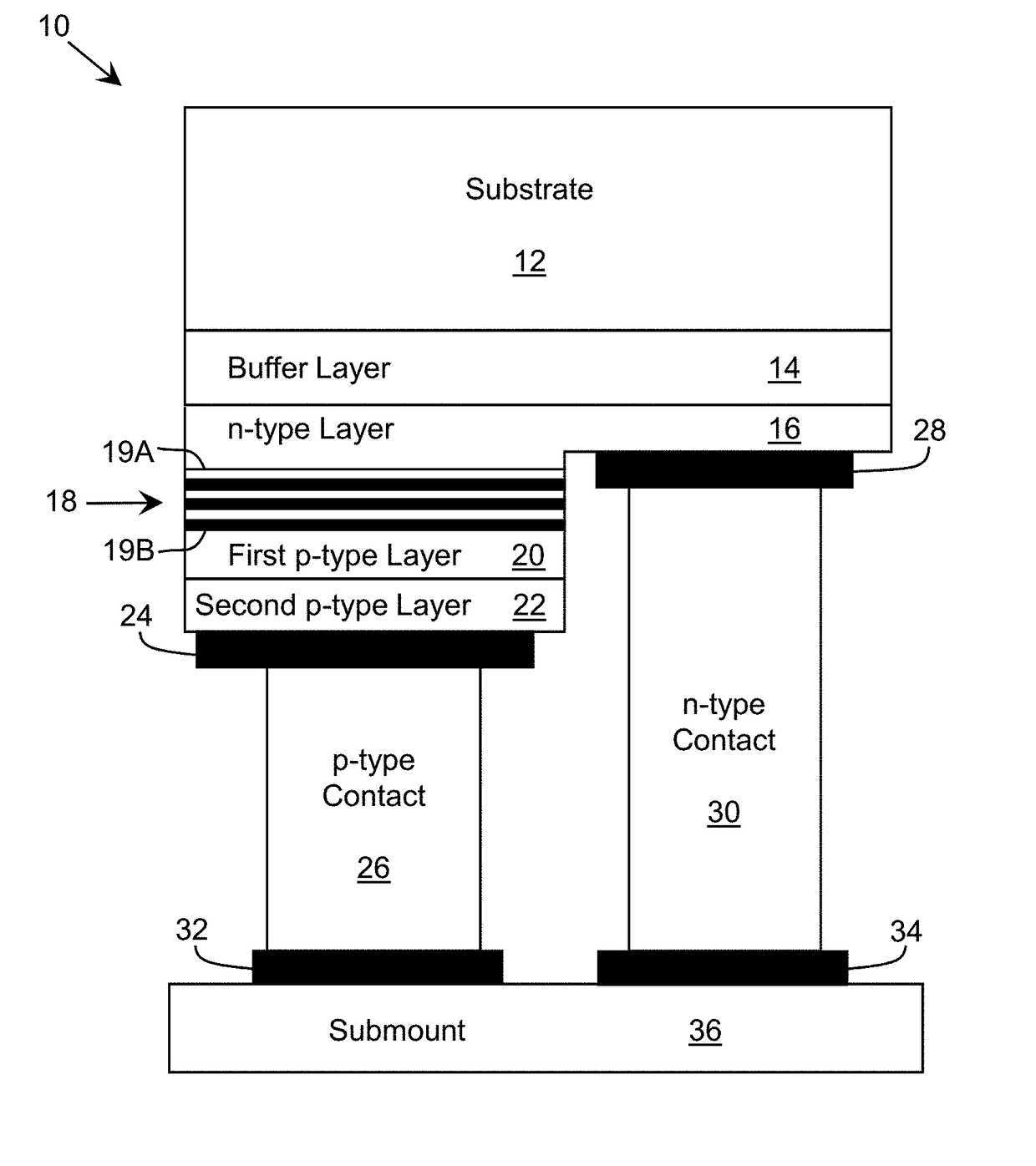
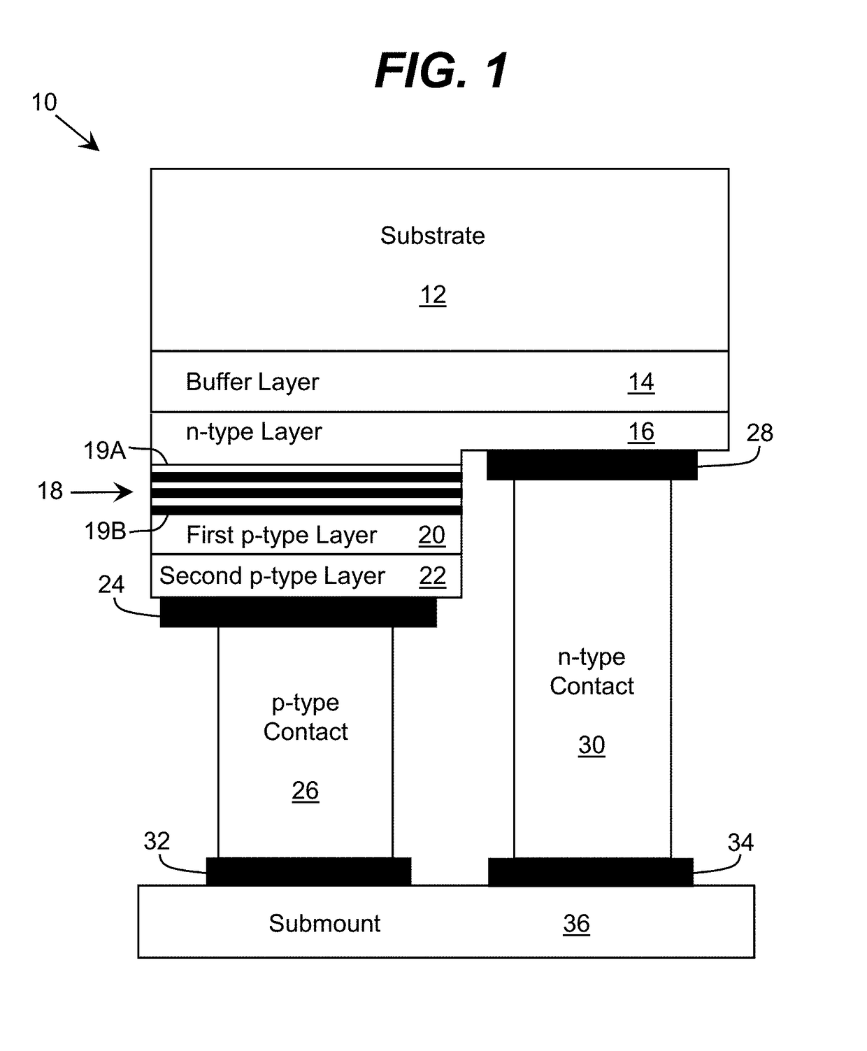
[0030]As indicated above, aspects of the invention provide an improved heterostructure for an optoelectronic device. The heterostructure includes an active region, an electron blocking layer, and a p-type contact layer. The p-type contact layer and electron blocking layer can be doped with a p-type dopant. The dopant concentration for the electron blocking layer can be at most ten percent the dopant concentration of the p-type contact layer. A method of designing such a heterostructure is also described.

[0031]As used herein, unless otherwise noted, the term “set” means one or more (i.e., at least one) and the phrase “any solution” means any now known or later developed solution. As used herein, two materials have comparable compositions when the molar fractions of the corresponding materials differ by at most ten percent (five percent in a more specific embodiment). For example, considering two group III nitride materials, AlxInyBzGa1-x-y-zN and Alx′Iny′Bz′Ga1-x′-y′-z′N, the two mat...


PUM


Abstract

An improved heterostructure for an optoelectronic device is provided. The heterostructure includes an active region, an electron blocking layer, and a p-type contact layer. The p-type contact layer and electron blocking layer can be doped with a p-type dopant. The dopant concentration for the electron blocking layer can be at most ten percent the dopant concentration of the p-type contact layer. A method of designing such a heterostructure is also described.

Description

REFERENCE TO RELATED APPLICATIONS[0001]The current application claims the benefit of U.S. Provisional Application No. 62 / 492,470, filed on 1 May 2017, and is a continuation-in-part of U.S. patent application Ser. No. 15 / 588,896, filed on 5 May 2017, which is a continuation of U.S. patent application Ser. No. 14 / 944,538, filed 18 Nov. 2015, which claims the benefit of U.S. Provisional Application No. 62 / 081,222, filed on 18 Nov. 2014, and is a continuation-in-part of U.S. application Ser. No. 14 / 475,638, filed on 3 Sep. 2014, which claims the benefit of U.S. Provisional Application No. 61 / 873,346, filed on 3 Sep. 2013, each of which is hereby incorporated by reference.TECHNICAL FIELD[0002]The disclosure relates generally to electronic and optoelectronic devices, and more particularly, to group III nitride based electronic and optoelectronic devices.BACKGROUND ART[0003]Development of group III nitride based electronic and optoelectronic devices with high efficiency and reliability dep...

Claims


Application Information

Patent Timeline
IPC IPC(8): H01L33/00H01L31/105H01L31/0352H01L31/0224H01L33/04H01L33/14
CPCH01L31/105H01L31/035236H01L31/022408H01L33/002H01L33/04H01L2933/0008H01L33/145H01L33/32H01L33/0025H01L33/025H01L33/06H01L33/14H01L31/03048H01L31/0352H01L31/109
Inventor JAIN, RAKESHSHATALOV, MAXIM S.DOBRINSKY, ALEXANDERSHUR, MICHAEL
Owner SENSOR ELECTRONICS TECH
Why Eureka
Try Eureka