Semiconductor device

a technology of semiconductors and devices, applied in galvano-magnetic devices, instruments, magnetic measurements, etc., can solve the problems of difficult offset cancellation and only slightly improved sensitivity, and achieve the effect of improving sensitivity

Active Publication Date: 2018-09-06
ABLIC INC
View PDF4 Cites 1 Cited by
  • Summary
  • Abstract
  • Description
  • Claims
  • Application Information

AI Technical Summary

Benefits of technology

[0015]It is therefore an object of the present invention to provide a semiconductor device including a vertical Hall element that is improved in sensitivity obtained by a current that flows in a direction parallel to a substrate and is capable of performing offset cancellation by the spinning current technique.
[0017]According to the present invention, the drive current supply electrode is larger in depth than those of the Hall voltage output electrode and the electrode isolation diffusion layers in the second conductivity type semiconductor layer. Consequently, when a current flows between two drive current supply electrodes, the current flows in the direction parallel to the substrate, and flows widely in the semiconductor layer in its depth direction. That is, the current flows over the entire region from the bottom portions of the electrode isolation diffusion layers to the bottom portions of drive current supply electrodes. The magnetic sensitivity of the Hall element can therefore be increased.

Problems solved by technology

The structure of Japanese Patent No. 5966060, however, has a problem given below.
In the structure of Japanese Patent No. 5966060, however, the width of the current that flows in the direction parallel to the substrate is small as described above, and as a result, the sensitivity is only slightly improved.
This means that it is quite difficult to perform offset cancellation in the structure of Japanese Patent No. 5966060 by the spinning current technique.

Method used


Image

  • Semiconductor device
  • Semiconductor device
  • Semiconductor device

Examples


first embodiment

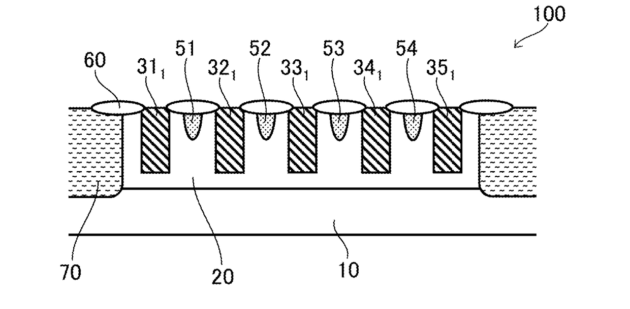
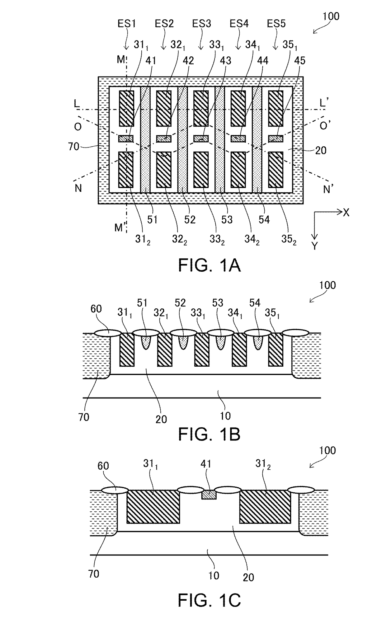
[0034]FIG. 1A to FIG. 1C are views for illustrating a semiconductor device that includes a vertical Hall element 100 according to a first embodiment of the present invention. FIG. 1A is a plan view of the semiconductor device, FIG. 1B is a sectional view taken along the line L-L′ of FIG. 1A, and FIG. 1C is a sectional view taken along the line M-M′ of FIG. 1A.

[0035]The semiconductor device of the first embodiment includes, as illustrated in FIG. 1A to FIG. 1C, a P-type (first conductivity type) semiconductor substrate 10, the vertical Hall element 100 provided on the semiconductor substrate 10, and a P-type element isolation diffusion layer 70 formed so as to surround the periphery of the vertical Hall element 100.

[0036]The vertical Hall element 100 includes an N-type (second conductivity type) semiconductor layer 20 formed on the semiconductor substrate 10, electrode sets ES1 to ES5 each of which includes a drive current supply electrode and a Hall voltage output electrode, and P-t...

second embodiment

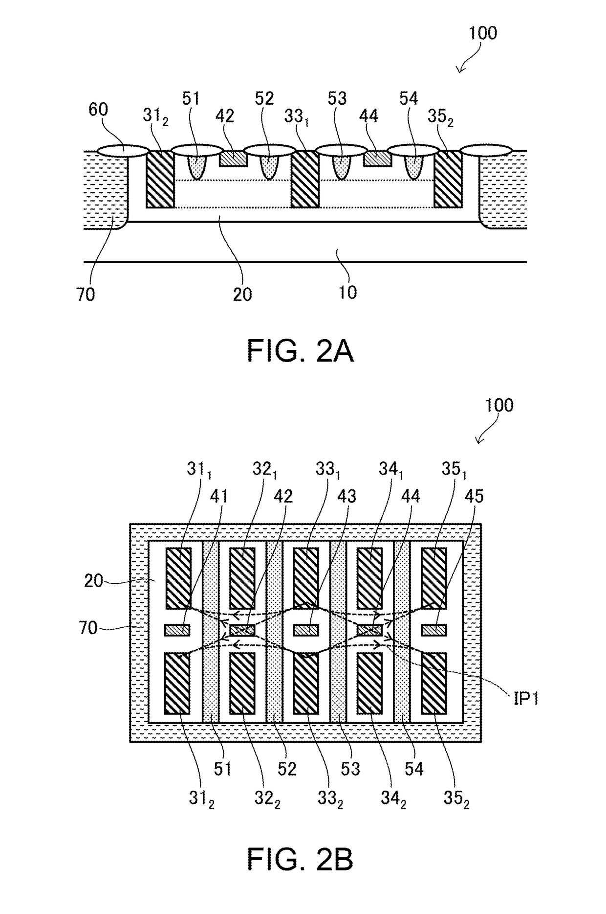
[0084]In the examples of the first embodiment described above, the drive current supply electrodes 31 to 35 have the concentration that is substantially equal to the concentration of the Hall voltage output electrodes 41 to 45, and have the depth that is different from that of the Hall voltage output electrodes 41 to 45.

[0085]In a second embodiment of the present invention, configuration of drive current supply electrodes is different from configuration of the drive current supply electrodes of the first embodiment described above.

[0086]For the purpose of easy understanding of the description, there is described an example in which the drive current supply electrodes 31 to 35 of the vertical Hall element 100 of the first embodiment illustrated in FIG. 1A to FIG. 1C are replaced with the drive current supply electrodes having the configuration according to the second embodiment.

[0087]FIG. 5A to FIG. 5C are views for illustrating a semiconductor device that includes a vertical Hall el...


PUM


Abstract

The vertical Hall element includes: a semiconductor layer of a second conductivity type formed on a semiconductor substrate of a first conductivity type; a first electrode set formed in a surface of the semiconductor layer and including a first drive current supply electrode, a Hall voltage output electrode, and a second drive current supply electrode aligned along a straight line extending in a first direction in this order; and second to fifth electrode sets each having the same configuration as the configuration of the first electrode set and aligned with the first electrode set along a straight line extending in a second direction perpendicular to the first direction. The Hall voltage output electrode has a first depth, the first and second drive current supply electrodes have a second depth that is larger than the first depth.

Description

RELATED APPLICATIONS[0001]This application claims priority under 35 U.S.C. § 119 to Japanese Patent Application No. 2017-039669 filed on Mar. 2, 2017, the entire content of which is hereby incorporated by reference.BACKGROUND OF THE INVENTION1. Field of the Invention[0002]The present invention relates to a semiconductor device, and more particularly, to a semiconductor device that includes a vertical Hall element configured to detect a magnetic field in a horizontal direction.2. Description of the Related Art[0003]A Hall element is capable of detecting position or angle without contact as a magnetic sensor, and accordingly has various uses. While magnetic sensors that use a horizontal Hall element configured to detect magnetic field components perpendicular to a semiconductor substrate surface (vertical magnetic field) are particularly well known, there have been proposed various magnetic sensors that use a vertical Hall element configured to detect magnetic field components paralle...

Claims


Application Information

Patent Timeline
Patent Type & Authority Applications(United States)
IPC IPC(8): H01L43/04H01L27/22H01L43/06
CPCH01L43/04H01L27/22H01L43/065G01R33/07H10N52/101G01R33/077H10B61/00H10N59/00H10N52/80
Inventor HIOKA, TAKAAKI
Owner ABLIC INC
Why Eureka
Try Eureka