Formulation for Deposition of Silicon Doped Hafnium Oxide as Ferroelectric Materials

a technology of silicon doped hafnium oxide and ferroelectric materials, which is applied in the direction of electrically conductive paints, chemical vapor deposition coatings, coatings, etc., can solve the problems of affecting the performance of ferroelectric materials in semiconductor applications, the dopant may not be homogeneous, and the loss of conventional ferroelectric materials

Active Publication Date: 2018-09-20
VERSUM MATERIALS US LLC
View PDF9 Cites 286 Cited by
  • Summary
  • Abstract
  • Description
  • Claims
  • Application Information

AI Technical Summary

Benefits of technology

[0022]In one aspect, the present invention is a composition for depositing a silicon doped hafnium oxide film comprising:(a) at least one organoaminosilane precursor compound having a formula of RxR3Si(NR1R2)3-x; where R is selected from halide (Cl, Br, I) or a linear or branched C1 to C6 alkyl; R1 and R2 are independently selected from linear or branched C1 to C6 alkyl wherein R1 and R2 are linked to form a cyclic ring structure or R1 and R2 are not linked to form a cyclic ring structure; R3 is selected from the group consisting of linear or branched C1 to C6 alkyl; x=0, 1, or 2; and (b) at least one organoaminohafnium precursor compound having a formula of LxHf(NR1R2)4-x wherein L is selected from cyclopentadienyl or alkyl substituted cyclopentadienyl; R1 and R2 are independently selected from linear or branched C1 to C6 alkyl wherein R1 and R2 are linked to form a cyclic ring structure or R1 and R2 are not linked to form a cyclic ring structure, x=0, 1 or 2. It is believed that having R3 group may reduce or increase the reactivity of organoaminosilane precursor towards to hydroxyl group, thus allowing better control of low level silicon doping into hafnium oxide.

Problems solved by technology

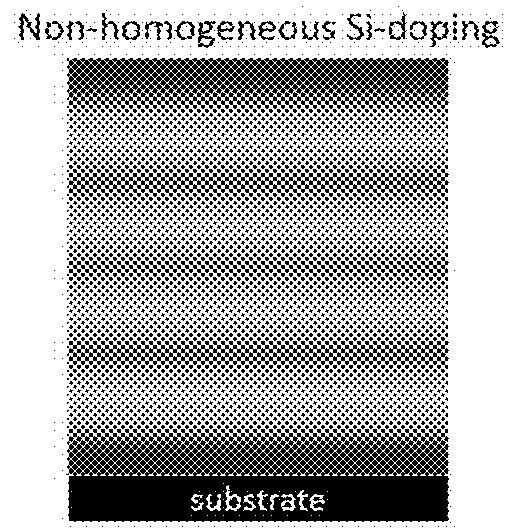
However, the silicon dopants may not homogenously distribute into the crystal lattice, which may be detrimental in the performance of ferroelectric materials in semiconductor applications.
However, these conventional ferroelectric materials suffer from various problems including poor Si-compatibility, environmental issues related to Pb, large phys. thickness, low resistance to hydrogen, and small bandgap.

Method used


Image

  • Formulation for Deposition of Silicon Doped Hafnium Oxide as Ferroelectric Materials
  • Formulation for Deposition of Silicon Doped Hafnium Oxide as Ferroelectric Materials
  • Formulation for Deposition of Silicon Doped Hafnium Oxide as Ferroelectric Materials

Examples


example 1

ALD Silicon Doped Hafnium Oxide Using about 4.4 wt. % of Bis(Dimethylamino)Dimethylsilane in a Formulation Comprising Bis(Dimethylamino)Dimethylsilane and Tetrakis(Dimethylamino)Hafnium and Ozone as Oxygen-Containing Source

[0150]The silicon wafer was loaded into the CN-1 reactor equipped with showerhead design with 13.56 MHz direct plasma and heated to 200° C., or 250° C., or 300° C. with chamber pressure of 1 torr.

[0151]4.4 wt. % of bis(dimethylamino)dimethylsilane in a formulation comprising bis(dimethylamino)dimethylsilane and tetrakis(dimethylamino)hafnium as the formulation was delivered using DLI into the reactor with a flow of 50 mg / min or 100 mg / min through an atomizer.

[0152]The ALD cycle was comprised of the process steps provided in Table 1 and uses the following process parameters:[0153]a. Introduce the formulation precursor to the reactor[0154]Argon flow: 1000 sccm[0155]Formulation precursor pulse: 1 to 5 seconds[0156]b. Inert gas purge[0157]Argon flow: 1000 sccm[0158]Pu...

example 2

ALD Silicon Doped Hafnium Oxide Using about 4.4 wt % of Bis(Dimethylamino)Dimethylsilane in a Formulation Comprising Bis(Dimethylamino)Dimethylsilane and Tetrakis(Dimethylamino)Hafnium and Water as Oxygen-Containing Source

[0166]The silicon wafer is loaded into the CN-1 reactor equipped with showerhead design with 13.56 MHz direct plasma and heated to 300° C. with chamber pressure of 1 torr.

[0167]About 4.4 wt % of bis(dimethylamino)dimethylsilane in a formulation comprising bis(dimethylamino)dimethylsilane and tetrakis(dimethylamino)hafnium as the formulation precursor is delivered using DLI into the reactor with a flow of 50 mg / min through an atomizer.

[0168]The ALD cycle is comprised of the process steps provided in Table 1 and uses the following process parameters:[0169]a. Introduce the formulation precursor to the reactor[0170]Argon flow: 1000 sccm[0171]Formulation precursor pulse: 1 to 5 seconds[0172]b. Inert gas purge[0173]Argon flow: 1000 sccm[0174]Purge time: 20 seconds[0175]c...

example 3

ALD Silicon Doped Hafnium Oxide Using about 4.4 wt. % of Bis(Dimethylamino)Dimethylsilane in a Formulation Comprising Bis(Dimethylamino)Dimethylsilane and Tetrakis(Dimethylamino)Hafnium and Oxygen Plasma as Oxygen-Containing Source

[0182]The silicon wafer is loaded into the CN-1 reactor equipped with showerhead design with 13.56 MHz direct plasma and heated to 300° C. with chamber pressure of 1 torr.

[0183]About 4.4 wt % of bis(dimethylamino)dimethylsilane in a formulation comprising bis(dimethylamino)dimethylsilane and tetrakis(dimethylamino)hafnium as the formulation precursor is delivered using DLI into the reactor with a flow of 50 mg / min through an atomizer.

[0184]The ALD cycle is comprised of the process steps provided in Table 1 and uses the following process parameters:[0185]a. Introduce the formulation precursor to the reactor[0186]Argon flow: 1000 sccm[0187]Formulation precursor pulse: 1 o 5 seconds[0188]b. Inert gas purge[0189]Argon flow: 1000 sccm[0190]Purge time: 20 second...


PUM

PropertyMeasurementUnit
melting pointaaaaaaaaaa
temperatureaaaaaaaaaa
diameteraaaaaaaaaa

Abstract

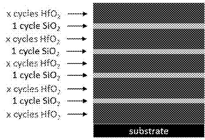
In one aspect, the invention is formulations comprising both organoaminohafnium and organoaminosilane precursors that allows anchoring both silicon-containing fragments and hafnium-containing fragments onto a given surface having hydroxyl groups to deposit silicon doped hafnium oxide having a silicon doping level ranging from 0.5 to 8 mol %, preferably 2 to 6 mol %, most preferably 3 to 5 mol %, suitable as ferroelectric material. In another aspect, the invention is methods and systems for depositing the silicon doped hafnium oxide films using the formulations.

Description

CROSS-REFERENCE TO RELATED APPLICATIONS[0001]This patent application is a non-provisional of U.S. provisional patent application Ser. No. 62 / 471,647 filed on Mar. 15, 2017 and 62 / 477,812 filed on Mar. 28, 2017, which are incorporated herein by reference.FIELD OF THE INVENTION[0002]The invention relates to formulations which can be used to deposit silicon doped hafnium oxide as ferroelectric materials for electrical memory applications.BACKGROUND OF THE INVENTION[0003]Described herein are novel formulations or compositions (they are exchangeable), methods, and systems comprising same to deposit silicon doped hafnium oxide via a thermal atomic layer deposition (ALD) or plasma enhanced atomic layer deposition (PEALD) process, cyclic chemical vapor deposition, plasma enhanced cyclic chemical vapor deposition or a combination thereof.[0004]More specifically, described herein is a composition, method and systems for formation of a silicon doped hafnium oxide having a silicon doping level ...

Claims


Application Information

Patent Timeline
Patent Type & Authority Applications(United States)
IPC IPC(8): H01L21/02C09D5/24C09D1/00C23C16/40C23C16/455C23C16/50
CPCH01L21/0228C23C16/405C23C16/45553C23C16/50H01L27/11507H01L28/40H01L21/02148C09D5/24C09D1/00H01L21/02274C09D7/40H01L21/02211H01L21/02219C23C16/401C23C16/45529C23C16/45531C23C16/45536C23C16/45527C23C16/45538H10B53/30
Inventor LEI, XINJIANMACDONALD, MATTHEW R.KIM, MOO-SUNGLEE, SE-WON
Owner VERSUM MATERIALS US LLC
Why Eureka
Try Eureka